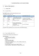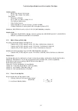
3.2
Technical Description
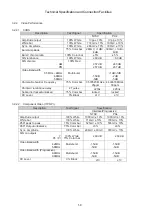
3.2.1 Audio
Performance
t
r
a
P
l
a
r
e
n
r
e
G
Output Stage Protection:
NA
Temperature :
Yes
Short Circuit:
Yes
s
r
o
t
a
c
i
d
n
I
e
v
i
t
c
A
y
a
l
p
s
i
D
k
c
o
l
C
:
r
o
t
a
c
i
d
n
I
e
d
o
M
y
b
d
n
a
t
S
f
f
O
s
n
r
u
T
D
E
L
:
e
d
o
M
y
b
d
n
a
t
S
r
e
w
o
P
Electrical Data
Normal
Limit
DSC: Y
Channel
Difference:
± 3dB
-
DBB: Y
Hum
(Vol
min
--- Vol
max
-20dB) 150nW
-
Bass:
NA
Residual Noise(Volume Minimum)
40nW
-
Treble:
NA
Channel Seperation: 1kHz/10kHz 40dB/35dB
%
0
.
1
%
8
.
0
l
a
m
i
x
a
M
,
D
H
T
A
N
:
s
s
e
n
d
u
o
L
Signal to Noise Ratio(A-weighted):
82dBA
77dBA
B
d
5
5
B
d
0
6
:
k
l
a
t
s
o
r
C
Amplification Reserve
3dB
2dB
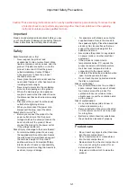
Audio Inputputs
Audio Input Sensitivity(± 3dB) rated output power at 1kHz
Audio Output(*1)
Tuner
FM 67.5kHz, Modulation (Limit:-6dB)
Line Out(Left/Right)
1000mV±200mV
CD/MP3
-3dB track (Audio Disc 1, Track 1)
Headphone
15mW ± 2 dB, RL
= 32Ω
)
S
H
0
.
2
(
e
v
a
w
e
n
i
s
z
H
K
1
B
d
3
-
B
S
U
AUX1(back)
1V; Rin ≥ 22kΩ
MP3_link(front)
500mV-1000mV; Rin ≥ 22kΩ
IPOD Docking
750mV; Rin ≥ 22kΩ
Output Power(*1)
At THD=10%, 1kHz
sinewave
MCD1060(ROP) MCD1060(Max
Power,30%)
(*2)
Main Operation for / all version (rms)
5W± 1dB
2x12W -1dB
( At Cold Condition with 10% THD )
Tuner output power(rms)
5W± 1dB
( At Cold Condition with 10% THD )
Frequency Response(± 3dB)
60Hz-20kHZ
Loudspeaker(Boxes): Separable speaker
box
Refer to package document of Speaker Box Assy
Speaker driver Impedance:
Right/Left:
4Ω @ 40 Hz ~ 20kHz(-3db)
:
r
e
f
o
o
w
b
u
S
REMARKS:
Electrical Parameters are to be measured at Speaker Terminals across rated impedance Load(6ohm) with
Rated Input Signal in CD Mode setting in DBB/Loudness Off and Pre-eq at Flat unless specified otherwise.
(*2)--- measure max volume power with 1V MP3-link input
Technical Specification and Connection Facilities
1-8
Summary of Contents for MCD1060/93
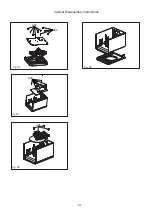
Page 24: ...8 2 Fig D3 Fig D5 Fig D4 Cabinet Disassembly Instructions Fig D6 A02 A03 A04 A02 ...
Page 28: ...Wiring Diagram Display Board Decoder Board AMP Board DVD Loader Power Board 11 1 11 1 ...
Page 31: ...AMP Board Layout Diagram 12 3 12 3 ...
Page 33: ...Display Board Layout Diagram 12 5 12 5 ...
Page 35: ...Power Board Layout Diagram 12 7 12 7 ...
Page 42: ...Decoder Board Layout Diagram 12 14 12 14 ...
Page 44: ...Revision List Revision List Version 1 0 Initial Release 14 1 ...

