


Circuit Descriptions, Abbreviation List, and IC Data Sheets
9.
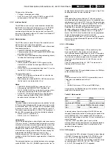
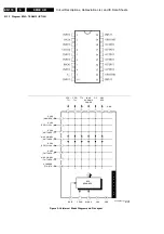
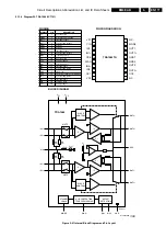
9.13.6
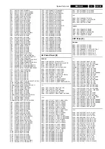
Diagram W, TDA1564 (IC7101)
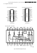
Figure 9-41 Internal Block Diagram and Pin Layout
BLOCK DIAGRAM
MGW244
+
−
+
−
+
−
+
−
MUTE
VI
VI
VI
IV
IV
VI
SLAVE
CONTROL
IN2
+
CIN
IN2
−
60
k
Ω
60
k
Ω
60
k
Ω
60
k
Ω
25 k
Ω
Vref
OUT2
−
OUT2
+
CSE
+
−
+
−
+
−
+
−
MUTE
SLAVE
CONTROL
IN1
+
IN1
−
OUT1
+
OUT1
−
+
−
VP
STANDBY
LOGIC
CLIP/PROTECTION
TEMP PREWARNING
MODE
OFFSET
DETECTION
DIAG
OC1
OC2
GND
VP2
VP1
TDA1564
CL 36532008_147.eps
140503
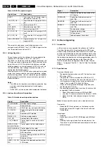
PIN CONFIGURATION.
TDA1564TH
IN1+
IN1-
CIN
CSE
MODE
OUT1-
OUT1+
GND1
OUT2-
OUT2+
OC2
DIAG
IN2-
IN2+
1
2
3
4
5
6
7
8
9
10
11
12
13
14
15
16
17
18
19
20
GND2
N.C.
N.C.
VP1
VP2
OC1
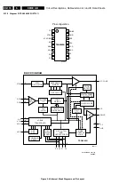
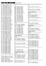
PINNING
SYMBOL
PIN
DESCRIPTION
n.c.
1
not connected
MODE
2
mute/standby/operating
OUT1-
3
inverting output 1
OUT1+
4
non-inverting output 1
GND1
5
ground 1
GND2
6
ground 2
OUT2-
7
inverting output 2
OUT2+
8
non-inverting output 2
OC2
9
offset capacitor 2
n.c.
10
not connected
VP2
11
supply voltage 2
OC1
12
offset capacitor 1
IN2-
13
inverting input 2
IN2+
14
non-inverting input 2
DIAG
15
diagnostic
CSE
16
electrolytic capacitor for SE mode
IN1+
17
non-inverting input 1
IN1-
18
inverting input 1
CIN
19
common input
VP1
20
supply voltage 1


