Circuit Descriptions and Abbreviation List
EN 122
9.
The +33V is the tuning voltage for the Tuner.
The +5VT is derived from the +8V with stabilizer 7912 (see
diagram A8), and is used to supply the tuner only.
SSB Supply
There are several voltages going to the SSB: +8V6, +5V2 and
+3V3.
The +5V2 and +8V6 (always present) come directly from the
Standby power supply.
The +3V3 is derived from the +5V with stabilizer 7910 (diagram
A8.)
9.3.4
Main Supply (Diagram A1)
The main power supply is able to deliver continuous power
between 100 W and 160 W.
Some important notes:
•
V
BAT
is not isolated from the main supply ('hot'.)
•
V
BAT
is alignment free.
Principle
The Main Power Supply, generates the 141 V (V
BAT
) and the
+/- 16 V for the audio part. It is based on the 'buck booster'
principle. A booster converter produces an output voltage
which can be greater than its input voltage. This is necessary,
in order to get a stable V
BAT
when AC Power is lower than
approx. 120 V AC.
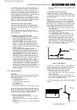
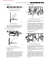
Figure 9-8 'Buck boost' principle
1.
After closing switch 'S', a linear in time increasing current
I
T
will flow through inductor L.
2.
Opening switch 'S' will generate a counter-e.m.f. in coil L,
trying to maintain the current. This is possible via diode D
(this diode is also called 'freewheel diode'.) Therefore, after
opening 'S', the magnetic energy stored in coil L will be
transferred to electrostatic energy in capacitor C.
3.
So, by changing the duty cycle, it will be possible to control
V
BAT
.
Implementation
At start-up of the main supply, C2515 (diagram A1) can be
assumed to be a short-circuit. U
AB
will be 15 V (R3513, D6510)
and U
GS
of the FET will be +5.4 V (via D6515.) The FET will be
driven into saturation (same as closing switch 'S'.) The drain-
current will increase linearly in time. With other words: resistors
R3513 and R3518 will start the oscillator.
The voltage across the co-coupled coil (4, 5) will keep the FET
in conductivity.
The TS7502 is a low-voltage semiconductor, which drives the
MOSFET TS7504. To bridge the different voltage levels, an
opto-coupler (item 7507) is used. Via this opto-coupler, the DC-
current through R3504 is influenced. The changed current
through R3504 changes the V
BE
of TS7502, which will
influence the drive of MOSFET TS7504 (= switch 'S' in figure
'Buck boost principle'.)
The sudden current interruption in the primary coil will induce a
counter-e.m.f. that tries to maintain the current via the
'freewheel' diode D6534. This current is linear decreasing in
time and, as it is also flowing through R3514//R3515, TS7502
will be blocked after a certain period. The gate of the FET will
be made positive again, is driven into conductivity, and the
cycle starts again.
For safety reasons, transistor TS7530 is added as a back-up
solution for TS7502. If B-E of TS7502 is shorted, TS7530 takes
over its function.
Stabilization of V
BAT
The output voltage V
BAT
is determined by:
V
BAT
= V
IN
* (T
ON
/ (T
ON
+ T
OFF
)) = V
IN
* duty-cycle.
To stabilize the output voltage, a feedback loop is
implemented, which will reduce T
ON
when V
BAT
increases and
vice versa.
Via a voltage divider, existing of (1 %) resistors R3507, R3510,
and R3527//3549, a voltage of 2.5 V (when V
BAT
= 141 V) is fed
to the input of precision shunt regulator 7506. This regulator will
conduct, and a current will flow through the diode part of the
opto-coupler 7507. The base of TS7502 will now be set at a
certain positive voltage. As this transistor switches the FET
TS7504 'on' and 'off,' this circuit can determine the duty-cycle.
For example, when the load increases, V
BAT
will decrease.
Consequently, the input voltage of regulator 7506 will
decrease, resulting in a lower current. Via opto-coupler 7505
and transistor TS7502, T
ON
of the FET is changed (will
increase.) The output voltage V
BAT
will rise.
If the load continues to increase, the regulator will block at a
certain moment. T
ON
is now at maximum value. This is the point
where V
BAT
will go below 141 V and, at further increasing load,
is switched 'off.' The voltage across the co-coupled coil (L5506,
pin 4 and 5) will decrease, due to the increasing load.
Therefore, the voltage on the gate of TS7504 comes below the
threshold voltage. The supply switches 'off,' and an audible
hiccupping can be heard.
On the other hand when the load decreases, V
BAT
will rise.
Consequently, the input voltage of TS7506 will also rise,
resulting in a higher current. This changes the base voltage of
TS7502, and through that the T
ON
of the FET will decrease. The
output voltage V
BAT
will be reduced.
If, for instance, V
IN
decreases (for example, U
MAINS
is 90 V i.s.o.
120 V), the slope of the drain-current will be flattened, through
which the FET will be in conductance longer, keeping V
OUT
constant.
If, for any reason, the stabilization circuit fails, the output
voltage V
BAT
can never exceed 200 V (via D6514.) D6514 will
form a short-circuit, V
BAT
will drop and the set will switch 'off'
(this will also result in an audible hiccupping of the supply.)
Switch to 'Standby' (via RC)
When the set is switched to 'Standby' mode via the Remote
Control, the Main supply is switched 'off' by the circuit around
TS7529 (see diagram A1.)
During 'on'-state, the Main supply is fed with line pulses via the
'SUP-ENABLE' line. They are rectified and smoothed via
D6517, D6516, and C2530, and fed to TS7529. Because they
are less than -20 V, this transistor is blocked. When these
pulses are stopped, TS7529 will be saturated and TS7502 will
switch 'on.' This will switch 'off' the Main supply.
It is important, that the Main supply is switched 'off' before the
Standby supply. This in order to prevent several unwanted
phenomena, such as audible plops and visible switch off spots.
Without an extra circuit to force this, this cannot be achieved.
Therefore, the circuit around TS7505 and TS7508 is
implemented.
This circuit compares the Main DC voltage (+375 V) and a
reference voltage (V
BAT
) via resistors R3554, R3555, R3560,
and R3556. Elcap C2539 serves as voltage source for the two
transistors.
CL 26532058_022.eps
100602
R
L
V
BAT
Vin
S
+
-
C
GND_SUP
L
GND_STB
+
D
www.freeservicemanuals.info
Summary of Contents for EM5A NTSC
Page 6: ...Direction for Use EN 6 EM5A NTSC 3 3 Direction for Use www freeservicemanuals info ...
Page 7: ...Direction for Use EN 7 EM5A NTSC 3 www freeservicemanuals info ...
Page 8: ...Direction for Use EN 8 EM5A NTSC 3 www freeservicemanuals info ...
Page 9: ...Direction for Use EN 9 EM5A NTSC 3 www freeservicemanuals info ...
Page 10: ...Direction for Use EN 10 EM5A NTSC 3 www freeservicemanuals info ...
Page 11: ...Direction for Use EN 11 EM5A NTSC 3 www freeservicemanuals info ...
Page 12: ...Direction for Use EN 12 EM5A NTSC 3 www freeservicemanuals info ...
Page 13: ...Direction for Use EN 13 EM5A NTSC 3 www freeservicemanuals info ...
Page 14: ...Direction for Use EN 14 EM5A NTSC 3 www freeservicemanuals info ...
Page 15: ...Direction for Use EN 15 EM5A NTSC 3 www freeservicemanuals info ...
Page 16: ...Direction for Use EN 16 EM5A NTSC 3 www freeservicemanuals info ...

