background image

Circuit Descriptions and Abbreviation List

EN 119

EM5A NTSC

9.

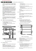
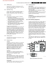
The RGB amplifiers on the CRT-panel are supplied with 200 V 
from the LOT.
The Auto-SCAVEM circuit modulates transitions of the 
Luminance (Y) signal on the horizontal deflection current, 
giving a sharper picture.
 
The sound part is built around the MSP34x2 (Multi-channel 
Sound Processor) for IF sound detection, sound control and 
source selection. Dolby decoding is also done by the MSP. 
Amplification is done via a 'class D' integrated power amplifier 
IC, the TDA7490.
 
The microprocessor, called OTC (OSD, TXT/CC and Control) 
takes care of the analog CC input processing and output 
processing. The OTC, ROM, and RAM are supplied with 3.3 V, 
which is derived from the +5V2.
The NVM (Non Volatile Memory) is used to store the settings, 
the Flash-RAM contains the set software.
 
There is a separate Standby Supply, in order to reduce the 
Standby power consumption. During Standby, the Main Supply 
is switched 'off' (via TS7529.) 
A relay (1550) is used to switch the Degaussing circuit. It is 
switched 'on' after set start-up and switched 'off' by the 

µ

P after 

12 s.
The Main Supply, a SMPS based on the 'boost-converter' 
principle, generates the 141 V (V

BAT

) and the +/- 16 V for the 

audio part. 
Note:
 Voltage V

BAT

 is not mains isolated ('hot'), but is alignment 

free.

9.3

Power Supply (Diagram A1 and A2)

The power supply has a number of main functions:
1.

Mains harmonic filter.

2.

Degaussing picture tube.

3.

Standby power supply.

4.

Main supply.

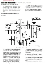
9.3.1

Mains Harmonic Filter (Diagram A1)

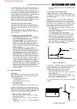
Figure 9-2 Mains harmonic filter circuitry.

The mains harmonic filter has two functions: to prevent high 
frequency signals (harmonics) from being transferred into the 
mains and to protect the set from lightning damage. 
 
C2507 prevents the high frequency signals generated by the 
set, from being conveyed into the mains (it forms a short-
circuit.)
 
In case of a lightning surge between the 2 phases (differential 
mode), the energy is immediately bled away through the VDR 
(R3509) to the other phase. 
In case of a lightning surge on both phases of the mains in 
relation to the aerial earth (common mode), the filter acts as a 
high resistance (U

EMK 

= L * dI/dt), as a result of which the 

voltage across coil L5503/04 increases. A spark gap (1590) 
prevents the voltage from increasing too much, which would 

lead to a damaged coil. When ignited, the current will be 
discharged via this spark gap. 
Resistor R3500 is used for limiting the inrush-current.

9.3.2

Degaussing (Diagram A1)

As soon as the set is switched 'on' via the ON/OFF switch, the 
5V2 is present. When the 'DEGAUSSING' signal from the 
processor (OTC) is 'low,' transistor 7528 will conduct, and relay 
1550 is activated. Initially a considerable current will flow, via 
PTC 3516, through the degaussing coil. The PTC will heat up, 
resistance will rise, and the current will decay rapidly. The OTC 
makes the 'DEGAUSSING' signal 'high' after 12 s, which will 
switch 'off' the relay.

9.3.3

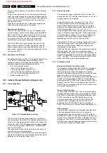
Standby power supply (Diagram A2)

Principle
This power supply is not only delivering the standby voltage, 
but also the main voltages for the small signal part. It is a SOPS 
type (Self-Oscillating Power Supply) and is regulated by the 
controlled switching of an oscillator. It uses the 'Flyback' 
principle:

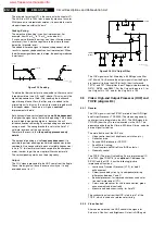
Figure 9-3 Flyback principle

After closing switch 'S,' the current I

D

 will increase linear in time. 

The magnetic energy in the primary coil is directly proportional 
with the self-inductance of the coil and current I

D

 (thus with the 

time the switch is closed.)
The voltage polarity at the secondary winding is negative (due 
to different winding direction), meaning that diode D will block. 
Capacitor C will discharge via R

L

, and U

OUT

 will decrease.

Opening switch 'S' will generate a counter-e.m.f. in the primary 
winding, trying to maintain current I

D

. Through this the polarity 

of the secondary voltage will inverse. The magnetic energy 
stored in the coil, will now be transformed to the secondary 
side. Diode D will now conduct, capacitor C will be charged and 
U

OUT

 will increase.

CL 16532044_020.eps

140501

2507

mains

3521
4M7

1501

1590

3501

9503

Mains harmonic

diversity

3551

2

1

3

4

V

9504

9504

+375V

-

-

+

2516

2537

3500

5502

5511 or 5516

3

1

1

2

4

3

2

5503 or

5504

96532156_020.eps

210100

+

-

-

+

-

-

+

+

RL

D

Id

Uout

C

+

C

+

375V

S

RL

D

Uout

375V

S

Isec

www.freeservicemanuals.info

Summary of Contents for EM5A NTSC

Page 1: ...m A6 46 51 57 Tuner SIMM connector Female Diagram A8 47 51 57 Receiver Diagram A9 48 51 57 Front Diagram A10 48 51 57 Inputs Outputs Diagram A11 49 51 57 Diversity Tables LSP 50 SIMM connector Male Diagram B1 58 68 77 IF I O Videoprocessing Diagram B2 59 68 77 PICNIC Diagram B3A 60 68 77 Diversity Tables SSB 61 68 77 Falconic Diagram B3B 62 68 77 Eagle Diagram B3C 63 68 77 HOP Diagram B4 64 68 77 ...

Page 2: ...Audio R 0 5 Vrms 10 kohm Audio out 1 Audio S 0 5 Vrms 10 kohm 2 Audio L 0 5 Vrms 10 kohm 3 Audio R 0 5 Vrms 10 kohm AV1 in 1 Y 0 7 Vpp 75 ohm 2 Pb 0 7 Vpp 75 ohm 3 Pr 0 7 Vpp 75 ohm AV1 in 4 Video 1 Vpp 75 ohm 5 Audio L 0 5 Vrms 10 kohm 6 Audio R 0 5 Vrms 10 kohm AV2 in 1 Video 1 Vpp 75 ohm 2 Audio L 0 5 Vrms 10 kohm 3 Audio R 0 5 Vrms 10 kohm AV2 in SVHS 1 Gnd 2 Gnd 3 Y 1 Vpp 75 ohm 4 C 0 3 Vpp 7...

Page 3: ...3 PWB location CL 26532058_010 eps 290502 TOP CONTROL PANEL MAINSWITCH PANEL LARGE SIGNAL PANEL SIDE I O PANEL CRT PANEL F O C N CO P E P A DAF PANEL I SMALL SIGNAL BOARD P B DC SHIFT optional G AUTO SCAVEM SC 3D COMB PANEL PIP DOUBLE WINDOW PANEL JACK HIGH DEFINITION INTERFACE www freeservicemanuals info ...

Page 4: ...ance inspection includes the following actions 1 Perform the general repair instruction noted above 2 Clean the power supply and deflection circuitry on the chassis 3 Clean the picture tube panel and the neck of the picture tube 2 3 Warnings In order to prevent damage to ICs and transistors avoid all high voltage flashovers In order to prevent damage to the picture tube use the method shown in Fig...

Page 5: ... best to test the high voltage insulation It is easy to do and is a good service precaution Before powering up the TV set with the back cover off or on a test fixture attach a clip lead to the CRT DAG ground and to a screwdriver blade that has a well insulated handle After the TV is powered on and high voltage has developed probe the anode lead with the blade starting at the case of the High Volta...

Page 6: ...Direction for Use EN 6 EM5A NTSC 3 3 Direction for Use www freeservicemanuals info ...

Page 7: ...Direction for Use EN 7 EM5A NTSC 3 www freeservicemanuals info ...

Page 8: ...Direction for Use EN 8 EM5A NTSC 3 www freeservicemanuals info ...

Page 9: ...Direction for Use EN 9 EM5A NTSC 3 www freeservicemanuals info ...

Page 10: ...Direction for Use EN 10 EM5A NTSC 3 www freeservicemanuals info ...

Page 11: ...Direction for Use EN 11 EM5A NTSC 3 www freeservicemanuals info ...

Page 12: ...Direction for Use EN 12 EM5A NTSC 3 www freeservicemanuals info ...

Page 13: ...Direction for Use EN 13 EM5A NTSC 3 www freeservicemanuals info ...

Page 14: ...Direction for Use EN 14 EM5A NTSC 3 www freeservicemanuals info ...

Page 15: ...Direction for Use EN 15 EM5A NTSC 3 www freeservicemanuals info ...

Page 16: ...Direction for Use EN 16 EM5A NTSC 3 www freeservicemanuals info ...

Page 17: ...loudspeaker cable from the subwoofer box while the set is operating because the class D amplifier cannot handle a change in load during operation There is no problem when the subwoofer is disconnected before operation but a change from connected to disconnected during operation can damage the amplifier 1 Disconnect the loudspeaker cable at the top of the subwoofer box 2 The subwoofer is fixed in t...

Page 18: ...ide the side that faces the tuner If you have to replace ICs you must take the complete SSB module out of the SIMM connector Note For access to the A side it is necessary to remove the Auto Scavem assembly at the left side of the SSB See the description in the Auto Scavem Assembly Panel section below To access the SSB test points do the following Figure 4 5 SSB removal part 1 1 Put the LSP in serv...

Page 19: ...he board by carefully releasing the four clamps 4 4 2 Side I O Assembly and Panel Figure 4 9 Side I O assembly 1 Release the snap hook 1 with your finger 2 At the same time pull the assembly backward 2 3 Release the two clamps on the right side of the bracket the board hinges at the left side 4 Remove the board from the bracket 4 4 3 AC Power Switch Assembly Panel Figure 4 10 AC Power Switch Assem...

Page 20: ...ket can be pulled out backwards 2 Release the two securing clamps 2 and lift the board out of the bracket 3 Both sides of the panel are now easy accessible 4 4 7 3D Comb Filter Assembly Panel This panel is placed in a bracket together with the 3D Comb Filter panel that is located on the left side of the tuner To remove the bracket 1 Pull the release handle 1 backwards This will lift the release ca...

Page 21: ...tly followed by MENU do not allow the display to time out between entries while keying the sequence Note It is possible that the main menu will appear when entering SDM To switch it off push the MENU button again Short the two pins on the external part of the SSB with the indication SDM Activation can be performed in all modes except when the set has a problem with the main microprocessor Caution ...

Page 22: ... control transmitter 123654 do not allow the display to time out between entries while keying the sequence Note Activation of the CSM is only possible if there is no user menu on the screen How to navigate Use the MENU UP DOWN keys on the remote control transmitter to navigate through the five CSM menus Contents of CSM Customer Service Menu 1 Software version example EM5US1_1 0_01234 Displays the ...

Page 23: ...L0R0 DD 2 1 DD 2 2 DD 3 0 DD 3 1 DD 3 2 DD 1 1 MPEG 1 0 MPEG 2 0 MPEG 2 0 LtRt MPEG 2 1 MPEG 2 2 MPEG 3 0 MPEG 3 1 MPEG 3 2 MPEG 1 1 or MPEG 2 2 Tuned bit Not applicable Surround Speakers Indicates if the surround speakers are set ON or OFF Change via MENU SETUP SPEAKERS and SURROUND SPEAKERS On Timer Indicates if the On Timer is set ON or OFF and if the timer is ON it also displays start time sta...

Page 24: ...ions ComPair consists of a Windows based faultfinding program and an interface box between PC and the defective product The ComPair interface box is connected to the PC via a serial or RS232 cable In the EM5 chassis the ComPair interface box and the TV communicate via a bi directional service cable via the service connector The ComPair faultfinding program is able to detect and diagnose problems o...

Page 25: ...ed errors since the last time the buffer was erased The buffer is written from left to right new errors are logged at the left side and all other errors shift one position to the right When an error has occurred the error is added to the list of errors provided the list is not full or the error is a protection error When an error occurs and the error buffer is full then the new error is not added ...

Page 26: ...ed Eagle Error error 27 at start up after initialization of the PICNIC the presence of the Eagle can be checked Table 5 3 Error Table Note Error codes 1 6 and 18 are protection codes and in this case supplies of some circuits will be switched off Also in protection the LED will blink the number of times equivalent to the most recent error code Error Device Description Def item Defect module indica...

Page 27: ...n special cases However in some error cases the microprocessor does not put the set in the protection mode this is the case with the hardware loudspeaker protection of the audio amplifier The content of the error buffer can be read via the service menu SAM the blinking LED procedure or via DST ComPair To get a quick diagnosis the EM5 has three service modes The Customer Service Mode CSM The Servic...

Page 28: ...S7442 is switched on and TS7443 is forced into conduction The SUP ENABLE signal is now shorted to ground level which will force the Main Power Supply to power off mode NON_VFB No vertical Flyback protection If the frame stage generates no pulses TS7641 will block TS7443 is now switched on which will lead to power off mode So in normal operation conditions TS7641 and TS7652 are conducting while TS7...

Page 29: ...orizontal amplitude in the SAM menu and remove the G S short of TS7480 5 8 5 Main Supply The simplest way to repair the main supply is to check and replace if necessary the gray marked components on the Main Supply This is the more detailed method 1 Replace FET 7504 and zener 6505 2 Remove the SSB panel 3 Short B and E of TS7529 in order to put the Main Supply in on mode TS7529 is then blocking Ca...

Page 30: ... operation you must check the RC receiver circuitry diagram E Relay degaussing is not au dible when set is switched from off or standby to on µP is not working correct ly When pin 115 is low the degaussing must be activat ed Check RESET circuitry on diagram B5 Check the level on pin 115 when you switch the set on Signal must initially be low and go to high after approx 12s No sound only picture Me...

Page 31: ...d 7723 Tip The whole Pixel Plus chipset 3 ICs 5 Field Memories can be diagnosed with ComPair No menu no OSD Probably a defective µP Measure around microprocessor on diagram B5 Various symptoms due to missing local supply voltage An interrupted fuse NFR re sistor or connection When no symptom or error code leads you to specific circuitry use the supply lines overview for a quick scan of all supply ...

Page 32: ...Service Modes Error Codes and Fault Finding EN 32 EM5A NTSC 5 Personal Notes www freeservicemanuals info ...

Page 33: ... 1735 1146 1417 1936 1499 1937 N C N C 1940 1737 8337 8338 1738 1953 1955 1205 80P TUNER TUNER 1943 compair interface LOT 12x CINCH 6x CINCH 1491 red 1417 1418 1693 1497 I 1435 SSB PANEL CRT PANEL F LSP LARGE SIGNAL PANEL 3P 3P 1933 4P 3P 3P 3P 3P 7P 1424 1680 1000 6P 1940 1956 5P 1303 9P 1382 5P 1951 4P 0207 3P 0236 5P 0200 5P 1104 5P 1947 5P 1946 1945 6P 0273 9P 11P 0201 10P 11P 7P 1304 5P 1303 ...

Page 34: ...41 3459 7455 8V6 13V LOT 15V_LOT ARC PROT 8Vb 8V6 6 5 5100 7103 OR 7104 7 8 10 3 6107 5103 6111 3113 6122 11V_STBY 11V 5 2V 5V 5 2V_MP 8V6 8V6 6103 6109 20V 5102 2102 2 1 3456 3404 3419 7440 B CURRENT SOURCE 6 2 1 3 HFB_X RAY PROT B4 B4 FRAMEDRIVE HOP B5 OTC STANDBY HOP HOP FRAMEDRIVE B4 FOCUS A 2 3 4 1 1495 3479 6491 EW 7442 7654 7653 3660 VBATT 3640 3631 8V6 6627 6626 6625 3642 3643 TV 3630 3632...

Page 35: ...TC 9 C FRONT IN FRONT DETECT VIDEO HIGH DEFINITION INTERFACE DUAL WINDOW PULSE FORMER 530us L1 L2 L3 L6 L4 12 14 15 19 18 Y OUT OUTPUTS 12 14 15 18 19 NOT USED IF EAGLE IS PRESENT U OUT V OUT VD HD OR OR OUTPUT FILTER OR OR OR 3721 HD100 VD100 OR OR OR OR 54 OR Y_EAGLE_E U_EAGLE_E V_EAGLE_E Y100 U100 V100 6 8 9 VD_E HD_E Y_EAGLE_E U_EAGLE_E V_EAGLE_E VD_E B3A PICNIC C1 DW PANEL B6 FALCONIC B3B B3C...

Page 36: ...L CONTROL AUDIO E TOP CONTROL P 79 78 37 77 SIM CONN B1 SIM CONN A8 66 65 1936 1936 2 2 1 3 4 5 6 7 8 9 2 1 3 2 GREEN IR RECEIVER 6051 TLUV5300 RED 1 3 4 5 6 7 8 9 3 1 1737 15W 8ohm SUBWOOFER 8 6 8 6 R L R L 5V2 23 A61 3 1 1738 5721 5720 5702 5701 15W 8ohm CENTRE 7678 A 12 13 14 14 7653 2 1 15 15 4 7653 5 3 61 7667 2 1 4 7652 5 3 OSC STBY MUTE 7702 TDA7490 PWM PMW 16V 19V 16V 19V 6 7 70 R CL_VL OU...

Page 37: ... SN DA E SN CL E SCL F 5V TUNER C2 3267 3268 4 5 7201 UV1316 AI 2 TUNER IF VIDEO SYNC C4 3330 3329 17 18 7301 TDA8885 BOCMA VCHIP PROCESSOR C5 3510 3509 15 14 7501 Z86130 V_CHIP NV ROM C6 3513 3512 6 5 7502 M24C32 NVM 3758 B53 B54 B51 B52 SDA S SCL S 3502 1955 4 1 2 1955 1 2 3500 3 7500 TDA8444T ERR 19 ERR 25 ERR 22 ERR 23 ERR 24 ERR 21 1951 1 2 DAC IIC Error Device Description Def item Defect mod...

Page 38: ... 3465 6464 6465 3464 3400 3305 3809 11VDC 3341 3301 3401 9401 5400 3404 3403 LINE OUTPUT STAGE 9410 5465 3 3463 3499 6462 3461 12 9 6460 11D TO 3450 3451 6400 FOCUS 2 FOCUS 1 EHT TO ANODE CRT 200V 6703 8Vvideo 8Vref 3460 5461 3462 3498 3635 5463 1485 6 FILAMENT 2 7 1424 1424 8 6463 3 1 3 1 FRAME DEFLECTION E W DRIVE A4 COLD HOT 3449 7620 TDA8177 4 2 11D 8Vb 13V LOT 13V LOT 8V S 141V 15V LOT 15V LO...

Page 39: ... div DC 5us div PM3394B A13 5V div DC 10us div PM3394B A14 200mV div DC 10us div PM3394B A17 20V div DC 5us div PM3394B A18 5V div DC 5us div PM3394B A19 1V div DC 5us div PM3394B A15 500mV div DC 5ms div A16 5V div DC 5ms div A22 1V div DC 10us div PM3394B A23 200mV div DC 10us div PM3394B A24 5V div DC 10us div PM3394B A25 2V div DC 10us div PM3394B A57 20V div AC 2us div PM3394B A59 10V div DC ...

Page 40: ...4B V9 2V div DC 200us div PM3394B V10 2V div DC 200us div PM3394B L4 1 V div DC 10ms div L5 1 V div DC 20µs div L1 1 V div DC 10µs div L2 1 V div DC 10µs div L3 1 V div DC 10µs div L6 500mV div DC 10us div PM3394B L7 500mV div DC 10us div PM3394B L9 1V div DC 250ns div PM3394B L10 1V div DC 20us div L11 1V div DC 5ms div B28 1V div DC 20 s div PM3394B B29 1V div DC 20 s div PM3394B V28 1V div DC 1...

Page 41: ...1 B1 9502 B1 9503 B3 9504 B3 9505 F5 2544 3553 7529 BC546B 2 1 3 GND SSP 9507 0R15 3542 TL431 7506 3516 1 2 3554 6M8 3507 160K 220p 2510 9505 DSP 1591 3562 100R 1 4 3 2 2506 STPS8H100 6536 TCET1103 G 7507 1500 SDDF 1 3 2 4 5 6 5518 9511 2528 1u 6523 BAS216 3500 1R 3514 4M7 3503 STPS8H100 6535 2m2 2511 3520 33K 4n7 2535 BAT254 6506 9504 9501 2502 10n 5K6 2527 470p GND SUP GND SUP 3506 BYD33D 6519 2...

Page 42: ... 6141 3115 22u 2115 STPS8H100 6107 1 2 3131 470R 680R 3109 5108 2145 150V 470p 2121 220n GND STB MP125 1148 1A25 BC337 25 7101 6148 BYV27 200 3167 680R 3155 100R 220R 3114 1K 3107 GND STB 10K 3126 2124 10u 10R 3121 GND SSP 9123 1146 1 2 3 4 5 MCL4148 6144 3153 4K7 100u 5131 A10 7133 BC857B 1K 3105 3156 100R BC557B 7105 3108 1m 2118 2104 2m2 GND SSP 3160 1K STP16NE06 7131 2162 1u 220n 2122 1N5062 C...

Page 43: ... D8 6414 G10 6415 H10 3442 F4 3443 F4 HOT COLD HOT COLD HOT 2488 B7 2492 C3 2494 A6 2495 A7 5424 E7 5425 C7 1491 RES CRT 5V2 TO 13V7 5402 A7 2425 B7 3445 F13 3446 F13 3447 F11 3448 H10 6463 A11 6464 B11 RES 6V6 6413 G10 6421 A7 6422 C7 3444 F12 6434 D8 6435 D8 6460 E12 6462 A11 6V6 LINE RES RES VDAF A4 46 FILAMENT PULSES 0V TO 5410 B5 0V 0V A8 20 6423 B8 L GND SUP 3498 6R8 2422 1u2 BZM55 C27 6410 ...

Page 44: ... 7483 E6 7486 F8 7487 F8 7611 A7 7612 D6 7613 A8 7614 C5 7620 B9 3657 C3 3658 C2 3659 C2 3660 B6 3661 C12 0V 1V6 RES 9481 F5 9482 F7 9483 E7 9499 F12 9620 B10 9622 B11 6618 A6 6619 C11 6620 A10 6621 A10 6622 B10 13V7 A8 10 7641 A12 7652 B12 7653 F12 7654 E12 9405 F3 RES 7V9 RES 3639 56K 1V2 3659 2K2 2621 6499 BZX384 C10 2620 220n 100n 2454 15n 2451 1m 3449 100R 3 2 1 8 4 8 4 3657 22K LM393D 7450 A...

Page 45: ... 0V1 2 3 6080 C2 6081 B3 6082 B2 6083 C4 1V3 4 1 2 3 4 D E 1601 A2 1620 C4 ROTATION CIRCUITRY B 3684 6K8 470R 3681 1620 EH B 1 2 3 3687 820R 125mA 1601 MP13 7680 TDA7052 1 Vp 4 3 6 2 7 5 8 BZM55 C15 6083 6081 BZM55 C15 2601 100n 6082 BAT254 3685 27K 3686 56K MCL4148 6080 3682 100K 3683 10K BC847B 7681 11V TILT 11V 11V BC368 7682 CL 26532067_036 eps 050602 A52 A53 ROTATION COIL DEFLECTION TO Person...

Page 46: ...2778 B4 CENTRE AUDIO AMPLIFIER R 2779 D1 2780 D4 2781 D4 2782 D6 2783 D9 2784 E6 2785 E9 2786 A2 2787 A7 2788 D1 2789 D1 2790 D1 2791 E9 2792 D9 2794 D6 2795 D6 2796 E6 2797 D9 2717 F3 2718 E2 2719 E4 2720 B2 3704 A5 3705 B2 3706 E5 3707 C5 2725 E8 2726 D2 2727 E2 A8 6 OV OV OV OV 2728 D2 2729 F2 2740 F8 2741 E7 2742 E7 2743 E7 2744 E8 2745 E8 2746 E8 2747 D9 2748 E9 2749 B8 2750 C8 2751 A8 2753 B...

Page 47: ...48 1 2 3 1200 TEDE9 AGC 1 AS 3 IF1 11 MB1 6 7 MB2 12 13 14 15 2 10n 2496 100K 3429 2483 4n7 6402 BAS316 3430 100K 3427 56K BZX384 C5V6 330K 3428 6401 5902 33u 7911 L78L05 GND IN OUT 5901 10u c001 1 2 3 3 EH B 1953 EH S 1943 1 2 9901 2 3 1955 EH B AUTO SCAVEM 1 9203 3999 1K 9903 3 EH B 1952 PIP US 1 2 9988 2948 100u 2914 10u 9215 EH B 1965 1 2 9904 9983 9987 2200 10u 10K 3939 100R 3201 9902 2u2 294...

Page 48: ...u 2900 CL 26532067_004 eps 120602 A71 Large Signal Panel Front 2V 3V1 3 2 1 0V 0V A8 24 3999 E1 1949 B2 TO SWITCH C D 9970 A3 9973 B3 NC 0V PANEL A8 31 NC 0V 1 1946 EH B 3 4 5 1 2 3 A 0241 A8 25 TOP CONTROL TACT A8 27 A8 24 A8 24 A8 27 5V2 3V3 E 1945 E3 1946 B2 1947 A2 D E A B 2 3 4 5 6 7 8 9 0V 8V2 B C FRONT A8 25 3V3 PANEL TO 0345 1 2 3 1947 1 2 9973 1945 9978 PH B 1949 1 2 9970 KEYBOARD ON OFF ...

Page 49: ...9 1901 A1 1902 A F9 1902 B E9 1902 C D9 1 1995 D1 1996 D1 3982 A4 3983 B5 3984 B5 3985 B5 3986 B6 3987 D5 3988 D5 3989 D6 3990 E4 3991 E5 3992 E5 3993 E5 3994 E6 3995 A2 2998 B2 2999 C2 1982 D9 1983 C1 1984 B9 1987 A2 1988 A2 A8 61 A8 62 1 2 3 4 5 6 7 8 9 1 2 3 4 5 6 7 8 9 1991 1900 K 3991 39K 1900 H 14 17 3988 1K 7995 BC847B 2985 330p 75R 3964 2993 100p 3972 1K 3992 330R 1K 3978 1989 7994 BC857B ...

Page 50: ...Bridge coil C934 01 5422 X X X X Bridge coil W7131 003 5422 X Bridge coil W7132 004 5430 X X LOT PSLOT 1392 9004E 5430 X X LOT PSLOT 1392 9005C 5430 X LOT PSLOT OV2076 DAF 5430 X LOT SLOT 1392 9012B 5466 X 18uH 5469 X X X X X Bead 100MHz 80ohm 6412 X X BAS316 6413 X X BAS316 6414 X MM3Z7V5 6414 X PDZ33B 6415 X PDZ15B 6415 X PDZ33B 6464 X X X X X BYW76 RAS15 10 6465 X BYV29X 500 L 7407 X X BC847B 2...

Page 51: ...Circuit Diagrams and PWB Layouts 51 EM5A NTSC 7 Layout Large Signal Panel Top Side CL 26532067_007 eps 050602 www freeservicemanuals info ...

Page 52: ... E9 2156 E9 2159 D9 2160 D9 2162 G9 2201 G1 2202 G1 2403 D2 2404 D2 2409 D3 2412 D3 2414 D3 2415 D3 2417 C3 2440 D2 2441 B2 2442 B2 2443 B2 2444 B1 2445 B1 2448 A5 2454 E2 2455 F3 2457 D1 2458 E3 2466 A5 2480 C5 2481 C5 2482 D5 2483 F2 2493 E2 2494 B3 2495 B4 2496 F2 2497 A5 2498 A5 2499 A5 2502 E7 2504 D8 2513 E7 2514 E7 2524 E7 2525 E8 2528 B9 2530 E8 2532 F7 2533 D6 2535 D6 2538 E7 2544 D7 2545...

Page 53: ...outs 53 EM5A NTSC 7 Layout Large Signal Panel Overview Bottom Side Part 1 CL 26532067_08a eps Part 2 CL 26532067_08b eps Part 4 CL 26532067_08d eps Part 3 CL 26532067_08c eps CL 26532067_008 eps 300502 www freeservicemanuals info ...

Page 54: ...54 EM5A NTSC 7 Circuit Diagrams and PWB Layouts Layout Large Signal Panel Part 1 Bottom Side CL 26532067_08a eps 300502 www freeservicemanuals info ...

Page 55: ...Circuit Diagrams and PWB Layouts 55 EM5A NTSC 7 Layout Large Signal Panel Part 2 Bottom Side CL 26532067_08b eps 300502 www freeservicemanuals info ...

Page 56: ...56 EM5A NTSC 7 Circuit Diagrams and PWB Layouts Layout Large Signal Panel Part 3 Bottom Side CL 26532067_08c eps 300502 www freeservicemanuals info ...

Page 57: ...Circuit Diagrams and PWB Layouts 57 EM5A NTSC 7 Layout Large Signal Panel Part 4 Bottom Side CL 26532067_08d eps 300502 www freeservicemanuals info ...

Page 58: ...G4 v8 G4 v9 G4 v10 G4 v11 G5 v12 G5 v13 G5 H A B C D E F G H v1 G3 v2 G3 v3 G3 v4 G3 v5 G3 B5 90 B6 98 1 10 11 9 8 7 5 4 3 2 6 12 13 14 15 1 10 11 9 8 7 5 4 3 2 6 12 13 14 B4 155 B2 150 F251 B4 67 F261 B6 101 F223 F260 F243 F208 TO 1205 A B C D E F G 5904 v20 v9 v52 100p 2901 2905 100p 9960 9922 100p 2906 9945 BZX384 C6V8 6956 9903 9932 72 73 74 75 76 77 78 79 8 80 9 9919 58 59 6 60 61 62 63 64 65...

Page 59: ...4 5311 B14 5312 F14 5401 D3 5402 E5 5403 H2 5404 B7 5405 B7 5406 E6 5408 C6 5409 G8 5411 C1 5415 A2 5416 A3 5417 G7 3V9 9413 2339 10p 100R 3381 100n 2411 HC 49 U 1305 4M433619 2K7 3434 2380 1p5 V8 3463 4K7 5405 6u8 7413 BFS20 10p 2383 2405 4n7 3412 2384 100n BC847BW 7404 1K 100n 2353 3462 1K5 9324 2316 100n 3374 100R 10p 2355 560R 3404 3373 100R 220R 3403 7402 2402 330p 1p5 2382 BC847BW 1K 3474 68...

Page 60: ...6 100 DI26 7 DI27 52 DO10 53 DO11 55 DO12 56 DO13 57 DO14 58 DO15 60 DO16 61 DO17 74 DO20 73 DO21 71 DO22 70 DO23 69 DO24 68 DO25 66 29 DI10 28 DI11 27 DI12 24 DI13 22 DI14 21 DI15 20 DI16 19 DI17 97 DI20 98 DI21 99 DI22 2 DI23 4 DI24 5 DI25 6 RES 100R 3754 2878 100n 3730 680R CX 5F 1701 12M RES 3737 1K 22p 2713 100n 2762 12p 2708 RES 1R 3753 2777 100n 100R 3710 5701 1u 3K3 3725 100p 2721 100K 371...

Page 61: ...100nF 2889 X 100nF 2890 X 100nF 2891 X 100nF 2892 X 100nF 2893 X 100nF 2894 X 100nF 2895 X 100nF 2896 X 100nF EAGLE B3C Item PixelPlus sets Non PixelPlus sets DESCRIPTION 2897 X 100nF 2898 X 100nF 3711 X 47kohm 3744 X 2 2kohm 3745 X 1kohm 3757 X 47ohm 3771 X 15ohm 3772 X 15ohm 3785 X 330ohm 3786 X 330ohm 3787 X 330ohm 3788 X 1 5kohm 3789 X 220ohm 3790 X 560ohm 3791 X 470ohm 3792 X 1kohm 3793 X 2 2...

Page 62: ...C1 3 YC2 4 YC3 5 YC4 6 YC5 7 YC6 8 YC7 9 YD0 119 118 YD1 YD2 117 YD3 116 YD4 115 YD5 114 YD6 112 YD7 111 YA0 45 YA1 46 YA2 47 YA3 48 YA4 49 YA5 50 YA6 51 YA7 52 YB0 159 158 YB1 YB2 157 YB3 156 YB4 155 YB5 154 YB6 152 YB7 151 1 VSS C2 15 VSS CLK 80 VSS D2 120 VSS DI 105 VSS E1 121 VSS E2 135 VSS F2 78 59 VSS FL VSS G1 81 VSS G2 99 VSS K 143 VSS S 28 WE B 146 WE D 106 113 VDD F 69 VDD G 90 VDD K 142...

Page 63: ...0n 100n 2822 3820 75R 100n 2847 2864 100n 100n 2734 2717 12p 2851 100n 7729 BFS20 2884 100n 10u 2770 100n 2774 5743 5726 2p2 2815 100n 2846 10R 2 7 100n 2855 9741 B 9747 75R 3822 6 8V_CON 75R 3823 9741 D 10R 4 5 9741 C 10R 3 7731 BFS20 100n 2712 2833 100n 47K 3711 100n 2857 2867 100n 82R 3807 100n 2811 560R 3790 3792 1K BFS20 7728 75R 3819 100n 2804 3821 75R 5738 2809 100n 150R 3800 2803 100n 470R...

Page 64: ... C B1 92 B9 167 B5 135 RES ONLY PTV B1 84 B5 142 B1 85 B3a 128 HOP B1 71 B1 74 B1 155 B3a 130 B5 120 B1 77 B5 92 B5 136 BZX384 C6V8 6322 6320 BZX384 C6V8 10p 2345 BZX384 C6V8 6321 6309 BAS316 V29 10p 2349 22K 3386 5303 100MHZ BAS316 6304 V24 19 YOUT 6u8 5301 12 2 10 23 24 1 SC 11 SCL 14 SDA 21 SOUT 8 UIN 17 UOUT 20 VCC 9 VIN 16 VOUT 6 YIN TDA9178 7302 3 AD1 4 AD2 5 AD3 7 ADR 22 CF 15 DEC 18 GND 13...

Page 65: ...1 0 T0 94 P1 1 T1 95 P1 2 T2 96 24 D3 23 D4 27 D5 31 D6 35 D7 34 D8 30 D9 81 DATA 73 EAn 80 FADING 82 FRAME 78 G 83 HSYNC 2 IREF 1 IREF_DEC 79 B 71 CASHn 72 CASLn 5 CVBS0 4 CVBS0_R 7 CVBS1 6 CVBS1_R 36 D0 32 D1 26 D10 22 D11 25 D12 29 D13 33 D14 37 D15 28 D2 A16 44 A17 63 A18 65 A19 47 A2 64 A20 66 A21 67 A22 68 A23 51 A3 53 A4 55 A5 57 A6 59 A7 61 A8 62 A9 SAA5801H 7001 45 A1 60 A10 58 A11 56 A12...

Page 66: ... 3578 I14 3579 I14 3601 D12 3545 A12 3546 D11 3547 B13 3550 E3 3551 D2 3552 I4 3553 I5 3554 I5 3555 J5 3556 B14 3557 C13 B1 106 RES 3558 D14 3559 E13 3560 E1 3561 E13 3562 E1 3520 C12 3521 E13 3522 F13 3523 A7 3524 A9 3525 A9 3526 A10 3527 B10 3528 C14 3529 E14 3530 E14 3531 C1 3532 B7 3533 B5 3540 A6 3544 B11 2678 C8 2679 G9 2680 G9 2681 E4 2682 E3 2686 F9 N C TUNER SIM CONNECTOR 2687 G10 2690 B6...

Page 67: ...IP FLOP ONE SHOT 11mS OPTIONAL Small Signal Board Headphone 100n 2521 3510 47K B6 162 B1 108 B1 107 2523 C2 2522 C3 3505 E3 B1 B10 2521 A1 2520 A3 2530 D2 2529 B2 A B C D E 3513 C1 3514 C1 3515 D3 3516 C1 7681 A C3 7681 B A3 7682 B1 2528 C1 7681 A NJM4556AM 3 2 1 8 4 3506 E3 3507 E3 3509 E2 3510 B1 2531 C2 2532 E2 2578 E4 2579 C4 3500 B3 3501 B3 3502 C3 3504 C2 1 2 3 C D 3512 B1 B6 161 100K 3515 2...

Page 68: ...3 3345 E3 3346 E3 3347 E3 3348 E3 3349 D2 3353 E3 3361 D3 3363 D2 3370 E2 3371 E2 3372 E2 3373 D1 3374 D1 3375 D1 3376 D2 3377 D2 3379 D1 3381 D1 3387 D2 3388 E3 3389 D1 3390 E3 3393 D2 3394 D2 3395 D3 3396 D2 3397 D2 3398 D2 3399 E3 3400 E3 3402 D2 3404 E1 3406 D1 3409 D1 3411 D1 3412 D2 3416 E1 3418 D1 3423 E1 3433 D1 3436 E1 3437 D1 3439 E1 3442 E2 3443 E2 3444 E2 3447 E2 3448 E2 3449 E2 3460 D...

Page 69: ...Circuit Diagrams and PWB Layouts 69 EM5A NTSC 7 Layout Small Signal Board Part 1 Top Side CL 2653041_41a eps 150402 PART 1 www freeservicemanuals info ...

Page 70: ...70 EM5A NTSC 7 Circuit Diagrams and PWB Layouts Layout Small Signal Board Part 2 Top Side CL 2653041_41b eps 150402 PART 2 www freeservicemanuals info ...

Page 71: ...Circuit Diagrams and PWB Layouts 71 EM5A NTSC 7 Layout Small Signal Board Part 3 Top Side CL 2653041_41c eps 150402 PART 3 www freeservicemanuals info ...

Page 72: ...72 EM5A NTSC 7 Circuit Diagrams and PWB Layouts Layout Small Signal Board Part 4 Top Side CL 2653041_41d eps 150402 PART 4 www freeservicemanuals info ...

Page 73: ...D4 3414 D3 3415 D3 3417 D4 3419 E4 3420 D3 3421 D4 3434 D4 3435 D4 3441 D3 3445 D4 3446 E3 3450 D3 3451 E4 3452 E3 3453 D2 3454 D2 3455 D2 3456 D3 3457 D3 3459 D2 3463 D3 3465 E2 3467 E2 3468 E3 3470 E2 3471 E2 3473 E4 3474 E4 3500 D2 3501 E2 3502 E2 3504 D2 3505 D1 3506 E2 3507 E1 3509 D2 3511 D2 3515 D2 3521 E1 3522 E1 3532 D1 3533 D1 3540 D1 3544 D1 3545 D1 3546 D1 3547 D1 3550 D1 3551 D2 3556 ...

Page 74: ...74 EM5A NTSC 7 Circuit Diagrams and PWB Layouts Layout Small Signal Board Part 1 Bottom Side CL 26532041_42a eps 150402 PART 1 www freeservicemanuals info ...

Page 75: ...Circuit Diagrams and PWB Layouts 75 EM5A NTSC 7 Layout Small Signal Board Part 2 Bottom Side CL 26532041_42b eps 150402 PART 2 www freeservicemanuals info ...

Page 76: ...76 EM5A NTSC 7 Circuit Diagrams and PWB Layouts Layout Small Signal Board Part 3 Bottom Side CL 26532041_42c eps 150402 PART 3 www freeservicemanuals info ...
Page 77: ...Circuit Diagrams and PWB Layouts 77 EM5A NTSC 7 Layout Small Signal Board Part 4 Bottom Side CL 26532041_42d eps 150402 PART 4 www freeservicemanuals info ...

Page 78: ...834 F10 5839 B7 5848 C5 5849 D5 5851 D5 5853 D5 6801 A11 6802 B3 6XXX A7 7801 D9 7802 C2 7803 G3 7804 B3 7805 A5 7806 A6 7807 E4 7808 F2 7809 G1 7810 G5 7824 D3 7828 D5 7829 A9 7832 A7 7871 B10 7874 B11 7876 A12 7891 H2 7892 B2 7893 B3 7894 A3 7895 D2 6XXX MCL4148 100n 2XXX 3XXX 3K3 3XXX 10K 3856 BC847BW 7895 10K 3857 4834 4K7 3858 4822 680R 3804 220R 3803 BC847BW 7806 3802 680R 3801 220R 4821 780...

Page 79: ...267 D3 3268 D3 3270 C2 5261 B1 7201 B4 F2 0255 1 F1 15 6 8 SCL 4 SDA 5 VSPLL 7 VST 9 VT 2 7201 TEDH9X700A AGC 1 AS 3 IF1 11 IF2 GND 10 12 13 14 5u6 5261 100u 2261 47n 2269 1n 2262 3270 4K7 3265 3K9 3263 100u 2265 3267 100R 10K 3264 SCL SDA AGC 33V IF TER 5VS 100R 3268 C 2 F1 1V div DC 20µs div CL 16532043_041 eps 190602 7201 TUNER TEDH9X700A Diversity Table C2 F2 200mV div DC 20 s div Personal Not...

Page 80: ... 15 Z 4 Z 7401 B HEF4053BT 6 E 10 S 16 Vdd 7 Vee 8 Vss Y0 2 7401 C HEF4053BT 6 E 9 S 16 Vdd 7 Vee 8 Vss 5 Y0 3 Y1 7401 A HEF4053BT 6 E 11 S 16 Vdd 7 Vee 8 Vss 12 Y0 13 Y1 14 Z 470R 3438 BC847BW 4437 7438 390R 3439 3437 4K7 RES 7435 390R 3436 4434 1SS355 6436 BC636 4K7 3434 4K7 3453 7434 4K7 3451 3452 4K7 3457 4K7 4K7 3456 100u 2434 100n 2436 100n 2431 100R 3432 2432 100n 3431 100R 2 3 4 5 6 7 8 9 ...

Page 81: ...10 VIDEO SIF 12 VP1 23 TDA8885 7301 C 63 DR 64 7301 A TDA8885 AGCOUT 7 DECBG 55 DECDIG 50 GND 6 IFIN1 1 IFIN2 2 IFVO 16 27 IFVO AUDOUT PLLIF 15 QSSO AMOUT 2351 10n 6u8 5352 RES 2350 2349 10n 3354 RES RES RES RES RES 3356 3353 RES 3355 RES 1SS355 6301 3352 4315 4314 3318 100R 3322 8K2 3321 10K 3390 470R 47p 2392 5351 15u 15u 2391 100p 2390 47p 5350 2393 1n 4M7 3328 4313 1 2 3 4 3389 4K7 3302 0207 2...

Page 82: ... A1 2502 B1 2503 B1 2504 C1 2505 C1 2506 B3 2507 A4 2508 C1 2509 C1 2511 B4 3501 A2 3502 A1 3503 B1 3504 C1 3506 B3 3507 A4 3508 B1 3509 A3 3510 A3 5501 B3 7501 A2 3510 100R 3509 100R DT 38 1501 32K768 2505 56p 2507 1u 3507 6K8 5501 6u8 100n 2511 3506 10K 2506 100n 2508 6n8 3504 6K8 2504 68n 2509 100n 3503 470R 2503 100n 2501 22p 2502 8p2 10M 3508 3501 470K 3502 10M 15 16 17 18 2 3 4 5 6 7 8 9 5VD...

Page 83: ...Circuit Diagrams and PWB Layouts 83 EM5A NTSC 7 Layout Double Window Panel Top View CL 16532043_096 eps 280601 www freeservicemanuals info ...
Page 84: ...84 EM5A NTSC 7 Circuit Diagrams and PWB Layouts Layout Double Window Panel Bottom View CL 16532043_095 eps 250601 www freeservicemanuals info ...

Page 85: ...D3 87 AGND4 97 AGND5 75 ALTF 46 AVDD1 53 AVDD2 81 AVDD3 5000 UPD64083GF 7023 3036 270R 330R 3020 F007 100K 3095 2043 47u 2031 100n BAV99 6000 180R 3096 F021 3056 1K 3055 220R 3016 33R 100n 2019 10u 2054 2036 1u 2018 150p 10u 2053 2017 150p 5024 BC857B 7001 330R 3073 2033 100n 22p 2063 22p 2068 3059 27K 5009 22u BAV99 6002 5025 5K6 3098 2046 47u 1K8 3097 5030 5029 6 7 8 9 2042 100n 1009 JL 1 2 3 4 ...

Page 86: ...014 C2 3015 C2 3016 C2 3017 C2 3018 C2 3019 C2 3020 C2 3021 C2 3022 C2 3023 C2 3024 C2 3025 C2 3026 C2 3027 C2 3028 C2 3029 C2 3030 C1 3031 C1 3032 C1 3033 C1 3034 C1 3035 C1 3036 C1 3037 C1 3038 C1 3039 C1 3040 C1 3041 C1 3042 C1 3043 C1 3044 C1 3055 C1 3056 B2 3057 B2 3058 B2 3059 B2 3060 B2 3061 B2 3065 B2 3067 B2 3068 B2 3069 B1 3071 B2 3072 B2 3073 B1 3074 A1 3076 B1 3077 B2 3082 B1 3083 B1 3...

Page 87: ...071 E1 3072 F2 3073 F2 3074 E3 3075 F3 3076 C3 3077 D3 GND KEYBOARD MAIN SWITCH PANEL 5V STANDBY RC5 RECEIVER 50Hz 60Hz GND KEYBOARD IR LED GND KEYBOARD 0345 OF KEYBOARD FROM TO FROM TO 107V 0V 0V 0V 0V 0V 0V 0V 0V 0V 0V 0V 4V8 3V 5V3 1 2 3 4 1 1946 OF 5V3 3V5 FROM TO OR AC RC5 TOP CONTROL 1V9 0V2 5V2 0V5 3V3 B C D E F A B C D E F 0201 A1 0202 A4 0240 B4 0241 C4 0245 E4 1050 C1 1051 A2 2051 C1 207...

Page 88: ...045 eps 180402 Layout AC Power Switch Panel Bottom Side CL 26532041_046 eps 180402 2070 A1 3050 A2 3051 A1 3054 A2 3061 A1 3070 A2 3071 A1 3072 A1 3073 A1 3074 A1 3075 A1 3076 A2 3077 A1 3078 A1 3079 A1 3081 A2 3082 A2 3083 A2 3084 A2 4000 A2 4001 A2 4002 A2 4003 A2 4004 A2 4007 A2 4008 B2 4009 A1 4010 A2 4011 A1 6053 A1 4001 3076 4007 3081 4002 4003 4000 4004 3083 3084 4010 3072 3071 2070 3078 30...

Page 89: ...41 F5 10 11 8 9 6 7 4 5 2 3 1 10 8 9 6 7 4 5 2 3 1 12 13 14 15 11 8V_ 12V G EHT INF SVM O R CRT 1237 E G13 1237 F F11 1237 G F11 1237 H H11 B C D E F G H I A B C D E F G H I 0031 C7 0033 E7 0035 A7 1237 A G14 1237 B G11 1237 C G13 1237 D E11 CRT THOMSOM B HFB_X RAY PROT 2V8 150V GND_RGB GND_RGB 1K5 3524 GND_RGB BAS321 6307 RES 3514 1K5 GND_RGB 3541 560R 3n3 2408 6302 BAS321 2 3 4 5 6 7 560R 3511 S...

Page 90: ... 3488 3426 D8 3427 C8 3428 B2 3429 E4 3448 A8 3449 A8 3450 B2 3451 B2 3452 D3 3453 D3 3454 C8 3455 E3 3456 E3 3458 B5 3460 B5 3470 C7 3471 B8 3472 A7 3473 A6 3356 E8 3410 A5 SCAVEM COIL TO 3411 B5 3412 B5 3413 C5 3416 A8 3417 B8 3420 C3 3421 C3 3422 B3 3423 B4 3424 B4 3425 B4 22n 2410 3413 820R 9406 3477 10R 3454 820R GND_X 3356 1K 3424 2M2 3421 470R GND_X GND_X 3427 2M2 BCP56 7429 BAS316 6410 341...

Page 91: ...3304 B2 3305 A4 3334 A4 3338 A3 3339 B2 3340 B2 3341 B1 3345 B1 3347 B4 3348 B4 3349 B4 3350 A2 3351 A1 3352 A2 3401 B2 3402 B1 3403 B2 3404 B1 3470 C2 3472 C2 3473 C3 3478 C2 3510 A2 3520 A1 3530 A2 3544 A1 5300 C1 5303 B4 5304 B2 5308 A4 5309 C1 5310 C1 5400 B1 5500 A4 5501 A3 5502 A3 6400 B2 6405 B2 6406 A2 6426 A2 6427 A1 6428 A2 7330 A2 7340 A1 7350 A2 9304 A2 9309 A1 9310 C1 9311 C1 9405 B4 ...

Page 92: ... 3504 A1 3505 A1 3506 A2 3507 A2 3508 A2 3509 A2 3511 A1 3512 A2 3513 A2 3514 A2 3515 A3 3516 A3 3517 A3 3518 A2 3519 A2 3521 A2 3522 A2 3523 A2 3524 A2 3525 A2 3526 A2 3527 A2 3528 A2 3529 A3 3531 A2 3532 A2 3533 A2 3534 A2 3535 A2 3536 A1 3537 A2 3538 A1 3539 A1 3540 A1 3541 A1 3542 A2 3543 A2 3999 A4 6301 A3 6302 A3 6303 A4 6305 A3 6306 A4 6307 A3 6401 C2 6402 C3 6403 C3 6404 C2 6407 A3 6408 C1...

Page 93: ...338 A7 2339 B7 2340 D7 2341 F5 VG2 CRT THOMSON 8V_ 12V G EHT INFO 2342 B9 2347 A13 2348 A13 2357 H10 2358 B13 2359 B13 2403 H8 2404 H8 2405 G7 3525 E3 3526 F4 3527 E4 3528 F4 3529 E4 3530 E5 3531 C3 3532 D4 3533 C4 2510 A10 2511 A10 3301 H5 3303 D1 3304 E1 3305 A12 3334 G12 3338 E10 3339 E10 TO 4V7 3V1 1V4 6V3 3340 D10 3341 H4 3345 G8 3346 G10 3347 H14 3348 G13 3349 G12 3350 D9 3351 E9 5309 H4 531...

Page 94: ... 2438 B4 2439 C8 3310 E8 3356 E8 1 2 3 4 5 6 7 8 9 1 2 3 4 5 6 7 SCAVEM TO 3410 A5 3411 B5 3412 B5 3413 C5 3416 B8 3417 B8 3420 C3 3421 C3 3422 B3 3423 B4 9316 B4 9405 E1 9406 B6 9407 E1 RES RES CRT AUTOSCAVEM 8 9 A B C D E A B C D E 1483 E8 2410 B4 2411 D2 2420 B4 2427 D8 2428 D8 2430 B2 2432 A3 2433 B3 2434 D5 2435 E5 2436 A5 2437 B4 56K 3412 RES 2430 3p3 68R 3451 3411 56K BAS316 6402 GND_X 2R2 ...

Page 95: ...2 3340 B2 3341 B1 3345 B1 3346 B4 3347 B4 3348 B4 3349 B4 3350 A2 3351 A1 3352 A2 3401 B2 3402 B1 3403 B2 3404 B1 3470 C2 3472 C2 3473 C3 3478 C2 3510 A2 3520 A1 3530 A2 3544 A1 5300 C1 5303 B4 5304 B2 5308 A4 5309 C1 5310 C1 5400 B1 5500 A4 5501 A3 5502 A3 6400 B2 6405 B2 6406 A2 6426 A2 6427 A1 6428 A2 7330 A2 7340 A1 7350 A2 9304 A2 9309 A1 9310 C1 9311 C1 9405 B4 9406 C2 9407 A4 9416 B1 9417 C...

Page 96: ...1 3504 A1 3505 A1 3506 A2 3507 A2 3508 A2 3509 A2 3511 A1 3512 A2 3513 A2 3514 A2 3515 A3 3516 A3 3517 A3 3518 A2 3519 A2 3521 A2 3522 A2 3523 A2 3524 A2 3525 A2 3526 A2 3527 A2 3528 A2 3529 A3 3531 A2 3532 A2 3533 A2 3534 A2 3535 A2 3536 A1 3537 A2 3538 A1 3539 A1 3540 A1 3541 A1 3542 A2 3543 A2 3999 A4 6301 A3 6302 A3 6303 A4 6305 A3 6306 A4 6307 A3 6401 C2 6402 C3 6403 C3 6404 C2 6407 A3 6408 C...

Page 97: ...A3 318 A1 1430 A3 2430 B3 2431 B4 2493 B2 1 2 4 3 9493 5493 CU15 68n 2493 BY228 20 6431 BYD33V 6433 2431 470p 6432 BYD33V 470p 2430 6430 BY228 20 2 MP 400mA 1430 5430 1 2 317 1 318 CL 26532041_034 eps 180402 I CL 26532041_049 eps 180402 317 A3 318 A2 1430 A2 2430 A2 2431 A1 2493 A3 5430 A1 5493 A3 6430 A2 6431 A2 6432 A2 6433 A2 9493 A3 Personal Notes www freeservicemanuals info ...

Page 98: ...7 1 2 15R 3807 3808 22R 3809 10R 3818 4K7 1K8 3832 9800 2890 270p 2812 10n 1419 1 2 7821 BC857B 7822 BC847B 7818 BC847B 3831 4K7 3833 4K7 3810 470K 7823 BC857B 9804 1492 1 2 3897 1R 1490 1 1418 1 2 CU15 5801 1 2 4 3 3811 4M7 3824 4K7 3816 4K7 2816 220p 2821 68n 1 2 4 3 BYD33V 6810 2322592 3899 CU15 5810 2824 10u 3898 2322592 3819 4K7 7820 BC847B 3820 3K3 3822 4K7 6812 BZX79 C22 STP3NB80 7810 2 1 3...

Page 99: ...3 2890 A3 2891 A3 2892 A3 3805 A3 3807 C3 3808 C3 3809 B3 3810 B3 3811 B3 3812 C3 3813 C3 3814 B3 3815 B3 3816 C3 3897 A2 3898 A3 3899 A3 3998 B1 5800 A2 5801 A1 5810 B2 6810 C2 6812 B3 7810 B3 9800 B3 9803 A2 9804 A2 9805 A3 Layout VDAF Panel Bottom Side CL 26532041_053 eps 180402 2818 B1 3818 B1 3819 A1 3820 A1 3821 A1 3822 A1 3823 B1 3824 B1 3826 B1 3827 B1 3828 B1 3830 B1 3831 B1 3832 B1 3833 ...

Page 100: ...01 B5 3102 I2 3103 C5 3104 D5 3105 D5 3106 D2 3107 E2 7106 F9 7107 F3 7108 B10 7109 C9 3112 D10 3124 F9 3125 F10 3126 B9 100n 2132 3111 10K 100K 3110 GND V PMBT2369 RES 4K7 3141 GND S 7108 1K 3101 7 VEE 1 5 2 4 3 GND S 7102 A 74HC4052D 6 8 GND 10 9 16 VCC 100n 2133 GND S 9105 GND V 2K2 3104 9104 2109 2u2 9100 3102 4K7 22K 3127 RES 4K7 3143 TDA8601T 15 FBI1 14 FBI2 13 FBO 9 GND 16 IOCNTR SEL 5 2 VI...

Page 101: ...9 D12 2930 F5 2931 G7 2932 I5 2933 I7 I A B B OUT N1 N1 N1 N1 N4 N1 N3 N1 SND2_L_IN FBL H OUT 1917 F1 1918 F1 1920 G1 1921 H1 1922 I1 1923 F8 1924 H8 N1 N1 N1 3 1993 B B1 1993 C C1 1994 A F1 1994 B H1 1994 C I1 2900 E4 10 11 12 13 10 11 12 AV4 YPbPr SELECTION TO CON 1304 TO CON 1680 GND C D E F G C D E F G H H I 1104 B13 1304 A13 1680 E13 1901 A1 1902 C1 1903 B1 1904 E1 1905 E1 1906 E1 1907 E3 190...

Page 102: ...x 910R 3428 GND V GND V 3407 1K3 10 9 TSH93 7400 B 7 4 11 GND V 820R 3401 3403 820R 8 4 11 100n 2404 2K7 3429 GND V 22u 2407 10 9 8 4 11 8Vvideo 2408 100u 470R 3424 GND V GND V 3K 3422 7452 BC847B 14 4 11 560R 3421 BAS316 6703 3426 1K 7450 B TSH93 1K8 3408 3409 1K5 3430 1K 8Vvideo 3401 A3 3402 A3 3403 A3 3404 A4 3405 B3 3406 B3 3431 C2 3430 A2 N1 N1 3429 F3 3428 F4 3427 F3 3414 D3 3415 D3 3416 D4 ...

Page 103: ...C1 7907 C1 7908 B1 7909 B1 9100 A1 9101 A1 9102 A1 9103 A1 9104 A1 9903 D2 9904 D1 9910 D1 9913 D1 CL 26532067_023 eps 300502 Layout HD Jack Panel Bottom Side 2400 A2 2403 A1 2404 A2 2703 A1 2704 A1 2705 A1 2706 A1 2713 A1 2714 A1 2715 A1 2900 C1 2901 C1 2904 B1 2905 B1 2906 C2 2907 C2 2908 C2 2910 C2 2911 C2 2912 C2 2913 C2 2916 D1 2918 D1 2920 C1 2921 C1 3401 A2 3402 A2 3403 A2 3404 A2 3405 A2 3...

Page 104: ...C DETECT L GND GND 16 9 Y C FROM TO 1936 OF LSP SSP GND SIDE I O 6808 BZX284 C6V8 GND_AUD GNDB GND_AUD GNDB GND_AUD 2807 220n 3999 150R GND_AUD 6804 BZX284 C10 6801 BZX284 C6V8 6806 BZX284 C10 3810 680K 3849 3K3 1803 6805 BZX284 C10 2804 100p 1805 2834 10n GNDB 3809 3829 120R GNDB RES SDM EMG_S 4804 GNDB GNDB GNDB 3811 GNDB 3846 10K 1 2 39K YKB21 5101A 1327 1 2 3 4 5 7 8 GNDB 2803 680p 3804 1K 381...

Page 105: ...00 A1 9800 B1 9802 A1 9803 A1 9810 A1 Layout Side I O Panel Bottom Side CL 26532041_055 eps 180402 2803 B1 2804 B1 2805 B1 2806 B1 2807 C1 2810 C1 2832 A1 2834 A1 2840 A1 2841 A1 3801 C1 3805 B1 3806 B1 3808 C1 3809 C1 3810 C1 3811 B1 3812 C1 3813 B1 3814 B1 3815 C1 3816 C1 3845 C1 3846 C1 3847 C1 3848 C1 3849 C1 4800 B1 4801 B1 4802 A1 4803 A1 4804 B1 6801 C1 6802 C1 6803 B1 6804 C1 6805 B1 6806 ...

Page 106: ...001 E1 3002 E1 3003 E1 3004 E1 GND_KEYBOARD 1 3007 E2 3008 D2 3009 E3 3010 D3 3011 E3 3012 C3 3013 C3 3999 D4 TOP CONTROL 2 3 4 A B C KEYBOARD FROM TO 3002 3K3 4006 0346 1 2 3 0345 1 2 3 3012 560R 3013 3001 390R 390R 3010 560R 4005 3008 270R 4003 4001 3011 620R 4002 4004 3009 1K1 3K3 3007 1PS76SB10 6005 3005 2K 1K5 3006 CHANNEL CHANNEL 1703 1705 1704 3004 1K5 MENU 3003 200R CL 26532067_042 eps 050...

Page 107: ...9009 2500 5u6 5601 22n 100R 3502 10p 22R 3238 10p 2502 BC857B 7204 9006 3054 1K 7028 BFS20 15K 3016 7006 BFS20 1 2 3 2K7 3014 7000 BC857B 1956 BC847B 7208 1K2 3224 3204 22K 6K8 3222 5K6 3012 68K 3030 GND_RGB 9001 1K8 3032 GND_RGB 47K 3216 BFS20 7016 470K 3214 680R 3210 2210 470n 7505 BFS20 1K5 3226 BC857B 7002 7004 BC857B SC4 SC6 1u 2022 22n 2012 3000 100R 100n 2010 3K3 3036 7018 BFS20 GND 9011 90...

Page 108: ...1 3080 B2 3082 B2 3084 A2 3086 A2 3088 B2 3090 A2 3091 A1 3092 A2 3093 A2 3094 A2 3096 A2 3106 A2 3108 A2 3110 A2 3112 A2 3114 A2 3116 A2 3118 A2 3120 A2 3121 A1 3122 A1 3123 A1 3124 A1 3125 A1 3126 A1 3127 A1 3128 A1 3129 A1 3130 A1 3131 A1 3132 A1 3133 A1 3134 A1 3135 A1 3136 A1 3137 A1 3138 A1 3200 A1 3202 A1 3204 A2 3206 A2 3208 A2 3210 A1 3212 A2 3214 A2 3216 A1 3218 A1 3220 A2 3222 A2 3224 A...

Page 109: ...described in the Service Modes Error Codes and Fault Finding section Menu navigation is performed with the MENU UP DOWN LEFT and RIGHT keys of the remote control RC transmitter Figure 8 1 Top view LSP 8 2 1 Vg2 Adjustment Method 1 with oscilloscope In the frame blanking period of the R G and B signals applied to the CRT the HOP video processor inserts a measuring pulse with different DC levels Mea...

Page 110: ...e screen at the horizontal center of the screen are of minimum width without visible haze 3 Adjust the DYNAMIC focus until the horizontal line at the center of the screen is of minimum width without visible haze 4 Check overall spot performance and repeat steps 2 and 3 to achieve the best result a compromise between minimal visible haze at the middle of the screen and sharp lines at the edges of t...

Page 111: ...in table White levels Table 8 2 Cathode parameter Table 8 3 White levels Method 2 without color analyzer If you do not have a color analyzer you can use the default values This is the next best solution The default values are average values coming from production statistics 1 Select Cathode and enter the value 15 for all picture tubes 2 Select a Color Temperature Cool Normal or Warm 3 Set the Red ...

Page 112: ...ent if necessary 4 Note If the horizontal linearity in wide screen mode is out of tolerance add a DC shift correction panel 3104 328 06230 to connector 1419 of the DAF panel diagram I On the DC shift panel cut diode 6433 for correction to the right or diode 6432 for correction to the left Caution Be sure to switch the set off first Never plug in a module that is not pre aligned in a set that is on...

Page 113: ...presence absence of these specific ICs or functions is made known by the option codes You can set the hardware related options via the SAM Alignments Options or Option Numbers menu You can set the software related options via the SAM Dealer Options menu Notes After changing the option s save them with the Store command The new option setting is only active after the TV is switched off and on again...

Page 114: ... 4 3 4 3 picture tube 16 9 16 9 picture tube CRT size 28 32 36 29 34 38 16 9 CRT size in inches for USA sizes differ 4 3 CRT size in inches Picture Rotation Yes Frame rotation circuitry present diagram A5 No Frame rotation circuitry not present Anti Moire filter Yes Feature present No Feature not present Video repro Featurebox type Eagle Eagle IC present PixelPlus 1050i 1250i Lightsensor Yes Featu...

Page 115: ... Off AP PAL 2 On Sum OB2 2 Virtual Rear Spkrs 0 Off 4 On 3 Cordless Rear Spkrs 0 Off 8 On EU 5 Virtual Dolby 0 Off 32 On 6 Subwoofer 0 not present 64 present 7 13 EPG Type EU only 0 Type 2 8192 Type 2C3 3 2 AV4 2fH 0 Off EU 4 On AP US Sum OB3 3 AV3 2fH 0 Off EU 8 On AP US 4 Dual Screen 0 None EU 16 PIP DS AP US 6 TXT EPG Dual Screen 0 Off AP US 64 On 8 Aspect Ratio 0 4 3 256 16 9 9 Tilt 0 Off 512 ...

Page 116: ...1 FL7 n a 2 FL8 n a 3 FL9 DAS n a 4 FL9 Monitor n a 5 FL10 n a 6 FL11 7 FL12 8 FL14 n a 9 PV02 Sum OB8 1 2 3 6 AVL 0 Off 64 On 8 Picture tube size 0 28 16 9 256 32 16 9 384 n a 512 36 16 9 768 29 4 3 1024 34 4 3 1280 38 4 3 2048 n a 9 10 11 12 Anti moire 0 Off 4096 On Menu name Subjects Options Physically in set Personal Options Blue Mute Yes Picture mute active if no picture detected No Noise if ...

Page 117: ...M interface I O and interface provisions for extended functions such as PIP The main functionalities of the SSB are the core TV functionalities being set control video and audio decoding feature box video featuring and sync geometry control The LSP single sided is built up very conventional with hardly any surface mounted components on the copper side The LSP has a very large hot part including bo...

Page 118: ...PICNIC are together with the sync signals from the PICNIC then fed to the HOP High end Output Processor This IC handles the video control and geometry part The RGB signals for CC OSD from the µP are also inserted via the HOP The video part delivers the RGB signals to the CRT panel and the geometry part delivers the H drive V drive E W drive and TILT drive signals Both deflection circuits are hot a...

Page 119: ...hases of the mains in relation to the aerial earth common mode the filter acts as a high resistance UEMK L dI dt as a result of which the voltage across coil L5503 04 increases A spark gap 1590 prevents the voltage from increasing too much which would lead to a damaged coil When ignited the current will be discharged via this spark gap Resistor R3500 is used for limiting the inrush current 9 3 2 D...

Page 120: ...now If the PICNIC cannot communicate with the ROM the watchdog will generate a reset pulse on pin 7 which will re start the cycle again If one of the power supplies is absent or too low then a safety problem can occur in some cases for example a too high temperature of the stabilizer To prevent this from happening the voltage dividers at the bases of the transistors TS7710 and TS7707 are calculate...

Page 121: ...gy is transferred to output U2 of the supply Diode D1 is blocked because U3 is lower than U1 Time t2 Q2 is switched off Time interval t2 t3 During this period the rest of the energy will be transferred to output U1 The two controllers the primary feedback for U1 and the secondary feedback for U2 all work independently The secondary voltage U2 is controlled by the on time of Q2 As soon as the load ...

Page 122: ...bilize the output voltage a feedback loop is implemented which will reduce TON when VBAT increases and vice versa Via a voltage divider existing of 1 resistors R3507 R3510 and R3527 3549 a voltage of 2 5 V when VBAT 141 V is fed to the input of precision shunt regulator 7506 This regulator will conduct and a current will flow through the diode part of the opto coupler 7507 The base of TS7502 will ...

Page 123: ...YNC sync pulses are also fed to the OTC for stable OSD and CC The RGB outputs 77 78 79 together with fading pin 80 are fed to the HOP The fading pin has a double function it is used for making a transparent menu and as a fast blanking signal for CC 9 4 2 I2 C Bus There are three I2C busses used Slow max 100 kHz hardware I2 C bus called I2 C1 used for the Tuner Fast max 400 kHz hardware I2 C bus ca...

Page 124: ...es reference number 1993 A B C YPbPr with sync on Y RGB with sync on green note cinch inputs are normally used for YPbPr input Video input D sub reference number 1990 YPbPr with sync on Y note D sub input is normally used for RGB inputs only RGB with sync on Green RGB with separate H and V Sync called VGA in 480p RGB output This RGB output of the board is signaled into the set HOP section of SSB B...

Page 125: ...ence for the synchronization A digital control circuit that is locked to the reference signal of the color decoder determines the start up of the sync Note If the crystal must be replaced you must use only the genuine replacement part This crystal is very precise if it is replaced by another type of crystal there may be no color because of a different capacity A sync separation circuit is integrat...

Page 126: ...igital YUV signals enter via FM4 and FM5 the Eagle IC This IC has the following functions Luminance Transient Improvement LTI Peaking Programmable number of lines Programmable number of pixels per line Demo mode split screen Improved color transients CTI and color enhancement TOPIC Improved vertical zoom The digital YUV signals from the Eagle go via a passive output filter to the HOP 9 8 3 PICNIC ...

Page 127: ... vertical CTI only horizontal Peaking both horizontal and vertical More pixels per line More lines per frame Better color representation for skin tones green and sky By means of over sampling the video signals get a sample frequency of 64 MHz a bandwidth of 20 MHz and 1680 pixels per line previously 32 MHz 10 MHz and 840 pixels line This requires two extra field memories MEM4 and MEM5 The Eagle ca...

Page 128: ...nals presented to the HOP come from the Eagle These three signals all have the same circuitry so it is only explained once for Y Figure 9 16 YUV Output Filter The YUV signals are first filtered by a 64 MHz passive filter L5739 with C s Because the output signals from the Eagle are too small to drive the HOP directly the circuit around TS7731 and TS7728 amplifies them The gain is determined by R379...

Page 129: ...pin 3 the E W drive signal is available Pin 4 is a feedback input for the EHT info and is used to prevent pumping of the picture The EHT also varies dependent on the beam current For example for wide screen without load this is 31 5 kV and with load 1 5 mA 29 5 kV Frame Rotation For frame rotation a control voltage from pin 25 of the HOP is used Frame rotation is only used in wide screen sets 9 9 ...

Page 130: ...NEDRIVE1 signal becomes low TS7409 and TS7408 will block The voltage polarity across the primary winding of L5410 will invert The positive voltage on the secondary winding will now drive TS7421 into conductivity Because of the storage time of the line transistor TS7421 L5410 cannot transfer its energy immediately to the secondary side This may result in high voltage peaks on the collector of TS740...

Page 131: ... R3431 and C2431 are placed parallel to L5421 See diagram Line deflection circuitry item 1 S correction Since the sides of the picture are further away from the point of deflection than the center a linear saw tooth current would result in a non linear image the center would be scanned slower than the sides To solve this the deflection current for the right side and left side is reduced C2433 is q...

Page 132: ...over zener diode D6622 8 2 V C2622 will be charged to 19 V 13 15 8 2 0 7 V During the flyback scan the change in current per time is much larger so a higher voltage is required The flyback generator will now generate a voltage of 13 V on pin 3 Added to the charge on C2622 this will give a flyback voltage of 32 V depending on the CRT size this value can differ The amplifier IC IC7620 pin 5 supplies...

Page 133: ... output of 2 x 15 WRMS to two full range speakers For the higher specified sets a subwoofer and center speaker are easy to implement by adding a second amplifier Principle Audio power amplifier systems have traditionally used linear amplifiers which are well known for being inefficient In fact a linear Class AB amplifier is designed to act as a variable resistor network between the power supply an...

Page 134: ...5 RGB signal path The RGB signals from the HOP are fed to three identical amplifiers TDA6118 on the CRT panel We will use one of them B connector 1940 pin 9 as an example for this description After emitter follower TS7506 the signal is fed to TS7507 and TS7508 This circuit sends the signal with the same DC voltage to the RGB amplifier IC7350 pin 3 In order to cope with the higher picture definitio...

Page 135: ... Scavem on the lowest signal levels noise while the clipper circuit items 7018 and 7020 always gives the same amount of Scavem above a certain level The levels at which this occurs are controlled by the DAC4 and DAC5 lines and are dependent on the noise meter reading in the Auto TV program The input signal enters this circuit at emitter follower 7022 and is strongly attenuated via voltage divider ...

Page 136: ...e alteration of the Scavem signal transistors 7427 and 7415 in stage A will conduct while 7428 and 7414 are blocked In stage B the positive pulse is inverted so transistors 7426 and 7412 will conduct while both 7423 and 7413 are blocked The Scavem current will now flow via transistor 7412 through the Scavem coil and then through 7415 During negative alterations the current will flow through transi...

Page 137: ...equirements a data slicer is built on the DW panel IC7501 Z86130 will decode the V Chip coding for the DW picture The source for decoding is made possible by the SEL_PIP_CVBS signal at the IO port of IC7301 pin 60 When this signal is low Tuner 1 Tuner 2 or AV CVBS is selected When this signal is high the external YUV is selected 9 18 5 Power supplies The power supplies used by the DW panel are fro...

Page 138: ...bars keeps the original aspect ratio ACI Automatic Channel Installation algorithm that installs TV channels directly from a cable network by means of a predefined TXT page ADC Analog to Digital Converter AFC Automatic Frequency Control control signal used to tune to the correct frequency AGC Automatic Gain Control algorithm that controls the video input of the feature box AM Amplitude Modulation A...

Page 139: ...r the LED OSD On Screen Display OTC On screen display Teletext and Control also called Artistic SAA5800 P50 Project 50 communication protocol between TV and peripherals PCB Printed Circuit Board PICNIC Peripheral Integrated Combined Network IC SAA4978 main IC for 100 Hz features and feature processing PIP Picture In Picture Progressive Scan Scan mode where all scan lines are displayed in one frame...

Page 140: ...204 FALREF 205 REFIN 206 WEYUV_G 207 VDDA 208 VDDC 1 VSS 2 VDDA 3 UVF0 4 UVF1 5 UVF2 6 UVF3 7 UVF4 8 UVF5 9 UVF6 10 UVF7 11 VSS 12 VDDC13 YF0 14 YF1 15 YF2 16 YF3 17 YF4 18 YF5 19 YF6 20 YF7 21 VSS 22 VDDC 23 VDDA 24 VSS 25 SNCK 26 SNRST 27 HD28 VD29 INTR1 30 VA 31 SNDA 32 HREF 33 TRST 34 TMS 35 VDDC 36 VDDC 37 VSS 38 VSS 39 VDDA 40 VSS 41 TDI 42 TDO 43 TCK 44 45 46 47 48 49 50 51 52 PHILIPS EAGLE...

Page 141: ...4 40433 47µF 20 25V 2400 4822 124 11575 47µF 20 160V 2401 4822 121 42077 6 8nF 10 400V 2402 2020 012 93596 22µF 20 250V 2403 4822 126 14494 22nF 10 25V 0603 2404 4822 126 14494 22nF 10 25V 0603 2412 3198 024 44730 47nF 50V 0603 2413 4822 124 12255 10µF 20 50V 2414 3198 024 44730 47nF 50V 0603 2415 4822 126 13883 220pF 5 50V 2417 4822 126 14076 220nF 20 25V 2419 4822 126 14237 470pF 10 2kV 2420 222...

Page 142: ...3158 5322 117 13021 47Ω 1 0 063W 0603 3159 4822 051 30103 10k 5 0 062W 3160 4822 051 30102 1k 5 0 062W 3161 4822 052 10101 100Ω 5 0 33W 3164 4822 117 13632 100k 1 0603 0 62W 3165 4822 051 30331 330Ω 5 0 062W 3168 4822 051 20472 4k7 5 0 1W 3169 4822 051 30102 1k 5 0 062W 3170 4822 117 12925 47k 1 0 063W 0603 3171 4822 116 52297 68k 5 0 5W 3172 4822 116 52297 68k 5 0 5W 3200 4822 117 11373 100Ω 1 08...

Page 143: ... 3790 4822 051 30272 2k7 5 0 062W 3791 4822 051 30272 2k7 5 0 062W 3792 4822 051 30103 10k 5 0 062W 3793 4822 051 30103 10k 5 0 062W 3794 4822 051 30103 10k 5 0 062W 3795 4822 051 30103 10k 5 0 062W 3796 4822 051 30272 2k7 5 0 062W 3797 4822 051 30272 2k7 5 0 062W 3798 4822 051 30153 15k 5 0 062W 3904 4822 052 10688 6Ω8 5 0 33W 3928 4822 051 30008 Jumper 0603 3938 4822 117 11373 100Ω 1 0805 3939 4...

Page 144: ...77 7641 5322 130 60159 BC846B 7652 5322 130 60159 BC846B 7653 5322 130 60159 BC846B 7654 4822 130 60373 BC856B 7680 4822 209 60956 TDA7052 N2 7681 5322 130 60159 BC846B 7682 5322 130 44647 BC368 7700 9322 163 86682 TDA7490L 7701 5322 130 60159 BC846B 7702 9322 163 86682 TDA7490L 7703 5322 130 60159 BC846B 7704 5322 130 60159 BC846B 7705 5322 130 60159 BC846B 7706 4822 130 60373 BC856B 7707 5322 13...

Page 145: ...2 126 11663 12pF 2707 4822 126 11663 12pF 2709 2238 586 59812 100nF 80 20 50V 0603 2710 2238 586 59812 100nF 80 20 50V 0603 2711 2238 586 59812 100nF 80 20 50V 0603 2712 2238 586 59812 100nF 80 20 50V 0603 2713 4822 122 33761 22pF 5 50V 2714 4822 122 33761 22pF 5 50V 2716 2238 586 59812 100nF 80 20 50V 0603 2717 4822 126 11663 12pF 2718 4822 122 33752 15pF 5 50V 2719 4822 122 33752 15pF 5 50V 2720...

Page 146: ...822 051 30102 1k 5 0 062W 3340 4822 051 30101 100Ω 5 0 062W 3341 4822 051 30101 100Ω 5 0 062W 3342 4822 051 30101 100Ω 5 0 062W 3343 4822 051 20683 68k 5 0 1W 3344 4822 051 30222 2k2 5 0 062W 3345 4822 051 30103 10k 5 0 062W 3346 4822 051 30333 33k 5 0 062W 3347 4822 051 30223 22k 5 0 062W 3348 4822 051 30222 2k2 5 0 062W 3349 4822 051 30472 4k7 5 0 062W 3350 4822 051 30102 1k 5 0 062W 3351 4822 0...

Page 147: ...2 117 13043 220Ω 1 0 063W 0603 3810 4822 051 30391 390Ω 5 0 062W 3811 4822 051 30759 75Ω 5 0 062W 3812 4822 051 30759 75Ω 5 0 062W 3813 4822 051 30391 390Ω 5 0 062W 3814 4822 051 30759 75Ω 5 0 062W 3815 4822 051 30759 75Ω 5 0 062W 3816 4822 051 30391 390Ω 5 0 062W 3817 4822 051 30759 75Ω 5 0 062W 3818 4822 051 30759 75Ω 5 0 062W 3819 4822 051 30759 75Ω 5 0 062W 3820 4822 051 30759 75Ω 5 0 062W 382...

Page 148: ... 50V 2390 4822 126 11785 47pF 5 50V 0603 2391 2020 552 94427 0603 50V 100poF 5 2392 4822 126 11785 47pF 5 50V 0603 2393 3198 016 31020 0603 25V 1nF 2401 3198 017 41050 0603 10V 1µF 2402 3198 017 41050 0603 10V 1µF 2403 3198 017 41050 0603 10V 1µF 2404 3198 017 41050 0603 10V 1µF 2405 3198 017 41050 0603 10V 1µF 2411 4822 124 40248 10µF 20 63V 2412 4822 126 13879 220nF 20 16V 2415 4822 126 13879 22...

Page 149: ...µH 5816 4822 157 11506 Bead 120Ω 100MHz 5818 4822 157 11506 Bead 120Ω 100MHz 5827 4822 157 11506 Bead 120Ω 100MHz 5834 4822 157 11506 Bead 120Ω 100MHz 5839 4822 157 11506 Bead 120Ω 100MHz 5848 4822 157 11506 Bead 120Ω 100MHz 5849 4822 157 11506 Bead 120Ω 100MHz 5851 4822 157 11506 Bead 120Ω 100MHz 5853 4822 157 11506 Bead 120Ω 100MHz 6412 4822 130 11397 BAS316 6415 4822 130 11397 BAS316 6801 4822 ...

Page 150: ...159 BC846B 7011 5322 130 60159 BC846B 7012 4822 130 42131 BF550 7015 5322 130 60159 BC846B 7016 4822 130 60373 BC856B 7017 5322 130 60159 BC846B 7019 9322 163 48668 LM809M3X 3 08 7020 5322 130 60159 BC846B 7021 4822 209 17398 LD1117DT33 7022 9322 160 50668 LD1117DT25 7023 9322 170 65671 UPD64083GF Mains Switch Panel E Various 0001 3104 303 37733 Tact switch 0151 4822 256 91766 LED holder 0170 4822...

Page 151: ... TDA6118JF N1 7350 9352 694 46112 TDA6118JF N1 7414 5322 130 62804 BCP53 7415 5322 130 63033 BCP56 7422 5322 130 42718 BFS20 7423 5322 130 60159 BC846B 7425 5322 130 42718 BFS20 7426 4822 130 60373 BC856B 7427 5322 130 60159 BC846B 7428 4822 130 60373 BC856B 7429 5322 130 63033 BCP56 7430 5322 130 62804 BCP53 7431 4822 130 60383 BF824 7432 5322 130 42718 BFS20 7500 5322 130 42718 BFS20 7502 4822 1...

Page 152: ...051 30681 680Ω 5 0 062W 3715 4822 051 30333 33k 5 0 062W 3716 4822 051 30223 22k 5 0 062W 3717 4822 051 30223 22k 5 0 062W 3718 4822 051 30273 27k 5 0 062W 3900 4822 051 30759 75Ω 5 0 062W 3901 4822 051 30759 75Ω 5 0 062W 3902 4822 051 30759 75Ω 5 0 062W 3903 4822 051 30101 100Ω 5 0 062W 3904 4822 051 30101 100Ω 5 0 062W 3905 4822 051 30102 1k 5 0 062W 3906 4822 051 30102 1k 5 0 062W 3909 4822 051...

Page 153: ...2W 3028 4822 051 30223 22k 5 0 062W 3030 4822 051 30683 68k 5 0 062W 3032 4822 117 12903 1k8 1 0 063W 0603 3034 4822 051 30222 2k2 5 0 062W 3036 4822 051 30332 3k3 5 0 062W 3038 4822 051 30561 560Ω 5 0 062W 3040 4822 117 12925 47k 1 0 063W 0603 3042 4822 051 30682 6k8 5 0 062W 3044 4822 051 30102 1k 5 0 062W 3046 4822 051 30102 1k 5 0 062W 3048 4822 051 30102 1k 5 0 062W 3050 4822 051 30561 560Ω 5...

Reviews: