EN 51
3139 785 33120
8.
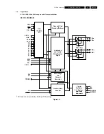
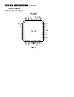
IC description
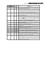
TERMINAL
TYPE
I/O
DESCRIPTION
NAME
PHP NO.
TYPE
I/O
DESCRIPTION
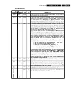
41
Supply
–
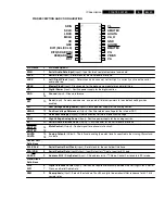
PLL circuit ground terminals. These terminals should be tied together to the
low-impedance circuit board ground plane.
40
Supply
–
PLL circuit power terminals. A combination of high-frequency decoupling
capacitors near each terminal is suggested, such as paralleled 0.1
µ
F and 0.001
µ
F. Lower frequency 10
µ
F filtering capacitors are also recommended. This supply
terminal is separated from DVDD and AVDD inside the device to provide noise
isolation. It should be tied at a low-impedance point on the circuit board.
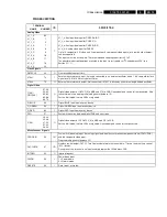
33
34
Bias
–
Current setting resistor terminals. These terminals are connected through an
external resistor to set the internal operating currents and cable driver output
currents. A resistance of 6.34 k
Ω ±
1.0% is required to meet the IEEE Std
1394-1995 output voltage limits.
37
CMOS
I
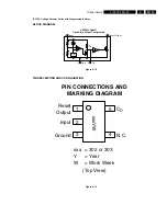
Logic reset input. Asserting this terminal low resets the internal logic. An internal
pullup resistor to VDD is provided so only an external delay capacitor is required for
proper power-up operation (see
power-up reset in the Application Information
section). The RESET terminal also incorporates an internal pulldown which is
activated when the PD input is asserted high. This input is otherwise a standard
logic input, and may also be driven by an open-drain type driver.
23
CMOS
I
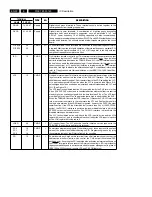
Test control input. This input is used in manufacturing test of the TSB41AB1. For
normal use this terminal may be tied to GND through a 1-k
Ω
pulldown resistor or
it may be tied to GND directly.
24
CMOS
I
Test control input. This input is used in manufacturing test of the TSB41AB1. For
normal use this terminal should be tied to GND.
1
CMOS
O
System clock output. Provides a 49.152-MHz clock signal, synchronized with data
transfers, to the LLC.
22
CMOS
I
Test control input. This input is used in manufacturing test of the TSB41AB1. For
normal use this terminal should be tied to VDD.
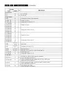
30
Cable
I/O
Twisted-pair cable A differential signal terminals. Board traces from the pair of
positive and negative differential signal terminals should be kept matched and as
29
Cable
I/O
positive and negative differential signal terminals should be kept matched and as
short as possible to the external load resistors and to the cable connector.
28
Cable
I/O
Twisted-pair cable B differential signal terminals. Board traces from the pair of
positive and negative differential signal terminals should be kept matched and as
27
Cable
I/O
positive and negative differential signal terminals should be kept matched and as
short as possible to the external load resistors and to the cable connector.
31
Cable
I/O
Twisted-pair bias output. This provides the 1.86 V nominal bias voltage needed for
proper operation of the twisted-pair cable drivers and receivers, and for signaling
to the remote nodes that there is an active cable connection.
PLLGND
PLLVDD
R0
R1
RESET
SE
SM
SYSCLK
TESTM
TPA+
TPA–
TPB+
TPB–
TPBIAS
XI
XO
42
43
Crystal
–
Crystal oscillator inputs. These terminals connect to a 24.576-MHz parallel
resonant fundamental mode crystal. The optimum values for the external shunt
capacitors are dependent on the specifications of the crystal used (see
crystal
selection in the Application Information section). When an external clock source is
used, XI should be the input and XO should be left open, and the clock must be
supplied before the device is powered on.

