ICD-MS525
AEP Model
UK Model
Tourist Model
SERVICE MANUAL
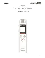
IC RECORDER
SPECIFICATIONS
Sony Corporation
Personal Audio Company
Published by Sony Engineering Corporation
9-877-928-01
2004E16-1
© 2004.05
Recording media
“Memory Stick“, Monaural recording
Recording time
Frequency range
SP: 120 Hz - 7,000 Hz
LP: 120 Hz - 3,500 Hz
Speaker
approx. 23 mm (
29
/
32
in.) dia.
Power output
200 mW
Input/Output
• Earphone jack (minijack) for 8 - 300 ohms ear
receiver/headphones
• Microphone jack (minijack, monaural)
Plug in power
Minimum input level: 0.7 mV 3 kilohms or
lower impedance microphone
• U SB connector
Playback speed control
+100% to -50% (DPC )
Power requirements
Two size AAA (LR03) alkaline batteries: 3 V DC
Dimensions
34.4 x 106.3 x 18 mm (1
3
/
8
x 4
1
/
4
x
23
/
32
in.)
(w/h/d) (not incl. projecting parts and controls)
Mass
75 g (2.7 oz) (incl. batteries and a “Memory Stick“)
Supplied accessories
“Memory Stick“ x 1
Application Software (CD-ROM) x
1
Ear receivers x 1
USB connecting cable x 1
Carrying case x 1
LR03 (size AAA) alkaline batteries x 2 (excluding
some areas)
Your dealer may not handle some of the above listed optional accessories.
Please ask the dealer for detailed information.
Design and specifications are subject to change without notice.
Maximum recording time of a “Memory Stick“*
The maximum recording time for all the folders are as follows. You can
record messages for the maximum recording time in a single folder.
16MB
32MB
64MB
128MB
SP**
2hr 10min.
4hr 24min.
8hr 52min.
17hr 47min.
LP***
5hr 47min.
11hr 45min.
23hr 38min.
47hr 26min.
(hr: hours /min.: minutes)
*
When using each “Memory Stick“ for use with ICD-MS525 only and by the
initial setting with three folders.
**
SP: Standard play recording mode (monaural sound)
*** LP: Long play recording mode (monaural sound)
Ver 1.0 2004.05