background image

EN 50

3139 785 33120

8.

IC Description 

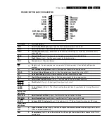
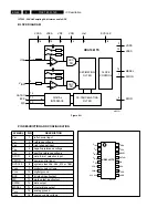
TERMINAL

TYPE

I/O

DESCRIPTION

PHP NO.

TYPE

I/O

DESCRIPTION

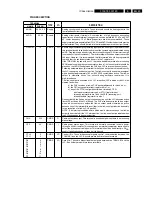
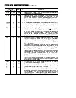
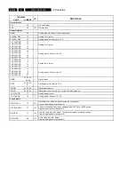
14, 46, 47

Supply

Digital circuit ground terminals. These terminals should be tied together to the
low-impedance circuit board ground plane.

21, 44, 45

Supply

Digital  circuit  power  terminals.  A  combination  of  high-frequency  decoupling
capacitors  near  each  terminal  is  suggested,  such  as  paralleled  0.1

µ

F  and

0.001

µ

F.  Lower  frequency  10

µ

F  filtering  capacitors  are  also  recommended.

These supply terminals are separated from PLLVDD and AVDD inside the device to

provide noise isolation. They should be tied at a low-impedance point on the circuit
board.

38
39

CMOS

I/O

PLL filter terminals. These terminals are connected to an external capacitor to form
a lag-lead filter required for stable operation of the internal frequency multiplier PLL
running from the crystal oscillator. A 0.1

µ

F

±

10% capacitor is the only external

component required to complete this filter.

19

CMOS

I

Link interface isolation control input. This terminal controls the operation of output
differentiation logic on the CTL and D terminals. If an optional Annex J type isolation
barrier is implemented between the TSB41AB1 and LLC, the ISO terminal should
be tied low to enable the differentiation logic. If no isolation barrier is implemented
(direct connection), or TI bus holder isolation is implemented, the ISO terminal
should be tied high to disable the differentiation logic. For additional information
refer to TI application note 

Galvanic Isolation of the IEEE 1394-1995 Serial Bus,

SLLA011.

13

CMOS

I

Link power status input. This terminal monitors the active/power status of the link
layer  controller  and  controls  the  state  of  the  PHY-LLC  interface.  This  terminal
should be connected through a 10-k

 resistor either to the VDD supplying the LLC,

or to a pulsed output which is active when the LLC is powered (see Figure 9). A
pulsed signal should be used when an isolation barrier exists between the LLC and
PHY. (See Figure 10.)
The LPS input is considered inactive if it is sampled low by the PHY for more than
2.6 

µ

s (128 SYSCLK cycles), and is considered active otherwise (that is, asserted

steady high or an oscillating signal with a low time less than 2.6 

µ

s). The LPS input

must be high for at least 21 ns to guarantee that a high is observed by the PHY.
When the TSB41AB1 detects that LPS is inactive, it places the PHY-LLC interface
into a low-power reset state. In the reset state, the CTL and D outputs are held in
the logic zero state and the LREQ input is ignored; however, the SYSCLK output
remains active. If the LPS input remains low for more than 26 

µ

s (1280 SYSCLK

cycles), the PHY-LLC interface is put into a low-power disabled state in which the
SYSCLK output is also held inactive. The PHY-LLC interface is placed into the
disabled state upon hardware reset.
The LLC is considered active only if both the LPS input is active and the LCtrl
register bit is set to 1, and is considered inactive if either the LPS input is inactive
or the LCtrl register bit is cleared to 0.

48

CMOS

I

LLC request input. The LLC uses this input to initiate a service request to the
TSB41AB1. Bus holder is built into this terminal.

16
17
18

CMOS

I

Power class programming inputs. On hardware reset, these inputs set the default
value of the power class indicated during self-ID. Programming is done by tying
these terminals high or low. Refer to Table 9 for encoding.

NAME

DGND

DVDD

FILTER0
FILTER1

ISO

LPS

LREQ

PC0
PC1
PC2
PD

12

CMOS

I

Power-down input. A high on this terminal turns off all internal circuitry except the
cable-active  monitor  circuits,  which  control  the  CNA  output  (64-terminal  PAP
package only). Asserting the PD input high also activates an internal pulldown on
the RESET terminal to force a reset of the internal control logic. (PD is provided for
legacy compatibility and is not recommended for power management in place of
IEEE 1394a-2000 suspend/resume LPS and C/LKON features.)

Summary of Contents for DVDR3465H/96

Page 1: ...aces 27 Layout Analog Main Part Top View 28 Layout Analog Main Part Bottom View 29 Front Front Panel Display 30 Front Front Panel Audio Video In 31 Layout Front Panel Top Copper Pattern SMD Components 32 Layout Front Panel Bottom Copper Pattern Components 32 Front Standby 33 Layout Standby Top View 33 Digital Back end Processor 34 Digital Memory 35 Digital IEEE 1394 Physical Layer 36 Digital Video...

Page 2: ...quency Response relative to 1 kHz 0 3 dB 100 Hz to 10 kHz S N unweighted 40 dB Quasi peak 22 Hz 22 kHz S N weighted 45 dB Quasi peak CCIR 468 Harmonic distortion at 1 kHz 1 5 FM 25 kHz Channel Separation 20 dB 1 3 4 Tuning Tuning Frequency Range 55 MHz 805 MHz Antenna Level for 40dB luminance S N video unweighted at 75Ω 40 dBμV High End 60 dBμV Low End Automatic Search Tuning Scanning time auto se...

Page 3: ... Hosiden According to IEC 933 5 Superimposed DC level on pin 4 load 100 kΩ 2 4V is detected as 4 3 aspect ratio 3 5V is detected as 16 9 aspect ratio Output Voltage Y 1Vpp 3dB Output Impedance Y 75Ω Output Voltage C 300mVpp 3dB Output Impedance C 75Ω OUT 3 COMPONENT VIDEO Cinch Y Pb Pr According to EIO 770 1 A EIA 770 2 A 1 5 Digital Inputs Outputs 1 5 1 DV IN IEEE 1394 Digital Video Input Impleme...

Page 4: ...te 95 dB during spin up spin down pause and access Outband attenuation 40 dB above 30 kHz 1 8 Dimension and Weight Set Dimension W x H x D 435 x 43 x 322 mm Net Weight 4 3 kg 1 9 Laser Output Power Wavelength 1 9 1 DVD Output power read mode 0 8 m W main beam Wavelength 658 nm at 25 C 1 9 2 CD Output power read mode 0 27 m W main beam Wavelength 785 nm at 25 C 1 10 Playability Video Playback 1 Pla...

Page 5: ...e kit ESD3 small tablemat wristband connection box extension cable and earth cable 4822 310 10671 Wristband tester 4822 344 13999 Be careful during measurements in the live voltage section The primary side of the power supply including the heatsink carries live mains voltage when you connect the player to the mains even when the player is off It is possible to touch copper tracks and or components...

Page 6: ...the adjusted temperature at the solder tip o To exchange solder tips for different applications Adjust your solder tool so that a temperature around 360 C 380 C is reached and stabilized at the solder joint Heating time of the solder joint should not exceed 4 sec Avoid temperatures above 400 C otherwise wear out of tips will rise drastically and flux fluid will be destroyed To avoid wear out of tips...

Page 7: ... B P R VIDEO CVBS COMPONENT VIDEO EXT 2 S VIDEO Y C VIDEO CVBS S VIDEO Y C AUDIO COAXIAL R L R L OUT 3 P R DIGITAL AUDIO INPUT OUTPUT OUT 2 OUT 1 EXT 1 AUDIO TV OUT ANTENNA IN AUDIO OUT L R VIDEO OUT Television rear Philips recorder rear To antenna or set top box VCR or similar device rear A Follow the steps A to E of Connecting under Basic Connections to connect the recorder before you proceed to...

Page 8: ...Shift Buffer TSB The TSB can store up to 6 hours of recordings temporarily Press DISPLAY once to display the Time Shift video bar 09 15 36 AM 08 30 45 AM 03 15 36 AM CH003 The TSB in playback mode Start time of program Program stored in TSB Shows TV channel or video input source TSB status icon in playback Time of current screen playback Current time The contents on the time shift buffer will be e...

Page 9: ... disc menu anytime For more recording and playback options see the accompanying User Manual Copying to a DVD recordable disc Types of discs used on this recorder You can copy the contents in your hard disk to a DVD recordable disc A Insert a recordable DVD disc B Press HDD to view the titles on the hard disk C Use up or down keys to select the title D Press SELECT to mark the titles you wish to co...

Page 10: ... The position numbers given here refer to the Exploded view on chapter 9 4 1 Dismantling of the DVD Tray Cover manually 1 Insert a screw driver into the slot provided at the bottom of the set and push in the direction as shown in Figure 4 1 to unlock before sliding the Tray Cover 110 out Figure 4 1 Unlock the Tray loader 2 Remove the Tray Cover 110 as shown in Figure 4 2 Figure 4 2 Remove Tray Cov...

Page 11: ... the Frontboard screw the Board ground connector to the chasis ground for ESD issue as shown in Figure 4 7 Figure 4 7 FrontBoard ground to Frame Ground 4 4 Dismantling of the Digital Board 1 Remove 4 screws to loosen the Digital Board 1013 as shown in Figure 4 8 Figure 4 8 Remove Digital Board Mounting screw 2 Service Position for Digital Board is given in Figure 4 9 Figure 4 9 Digital Board Servi...

Page 12: ...Board Service Position 4 7 Dismantling of the HDD 1 Remove 5 screws to loosen the HDD assembly HDD1006 HDD Bracket 185 Screws 269 Screws 270 Suspension Bracket 190 HDD Damper 191 as shown in figure 4 13 Figure 4 13 Remove mounting screws for HDD 2 Flip over the HDD Assembly to see the mounting screws 269 Remove the screws 269 to dismantle the HDD 1006 from the HDD Assembly Notes Only the special ty...

Page 13: ...ade 1 Open the tray and load the Upgrade CDROM 2 The tray closes and set will display FLASH1 3 The OSD will display Software Upgrade Disc detected Select OK to start upgrading or CANCEL to exit 4 Click on the OK button 5 The set will display Upgrading Software Please Wait Do not switch off the power It will do the Upgrade for the loader and OSD will show Loader Software Upgrade Loader Software Upg...

Page 14: ... set will display Load 6 Put the upgrade disc and close the tray and the set will show Copy Boot 7 The rest of the procedure follows the software upgrade given in 1B Procedure to apply the firmware upgrade Note 1 Do not press any button or interrupt the main supply otherwise the set may become defective 2 When the HDD formatting is successful the set will go to standby mode 5 3 Verification of Firmw...

Page 15: ...R VIA_SY_FR DAC AUD_DAT 0 AUD_WCK0 AUD_BCK0 14 12 11 9 ANALOG VIDEO 1109 CONTROL LINES CONTROL LINES SCK D_FM D_HOST RDY_FM ATN_FM HOST_RESET IDE BUS FAN 1112 IDE BUS OUT 2 DVD RW ENGINE TRAY CONTROL SERVO READ WRITE DISC HARD DISK POWER SUPPLY UNIT 40 40 LASER 1600 1 1571 AUDIO L R CONTROL AND COMMUNICATION LINES 1107 LOOP THROUGH CONTROL UNIT SLAVE MICROPROCESSOR UPD 16316GB 006 DIGITAL BOARD B ...

Page 16: ... V 5 5 N I S B V C F 5 D N G 6 2 9 D D 6 D N G 6 2 9 D D 6 D V 2 1 6 D N G 6 D N G 6 T S O H _ D 6 D N G 6 D N G 4 Y D R O I 7 2 5 D D 7 Y D R O I 7 2 5 D D 7 D N G 7 Y D 7 K C M A 7 D N G 7 T S R T S O H 7 N I L U A F 3 L E S C 8 2 0 1 D D 8 L E S C 8 2 0 1 D D 8 D N G 8 D N G 8 D N G 8 K C S P F 8 U C M _ N T A 8 D N G 2 N K C A M D 9 2 4 D D 9 N K C A M D 9 2 4 D D 9 D V 5 9 C D 9 K C B D 9 M F...

Page 17: ...iagrams Waveforms Wiring Diagram Waveforms Waveforms of Analog Board I143 Y_OUT I142 C_OUT I144 CVBS_OUT I137 D_C I138 D_SY I139 D_Pr I140 D_CY I141 D_Pb I241 Audio L out I242 Audio R out I150 DIGITAL_OUT I311 XTAL IN I312 XTAL OUT ...

Page 18: ...UD_BCKI T537 AUD_BCKO T541 AUD_DAI 0 T539 AUD_DAO 0 T543 AUD_MCKI T540 AUD_MCKO T544 AUD_WCKI T538 AUD_WCKO T542 VOA_RPr T521 VOA_BPb T518 VOA_CVBS T524 VOA_GY T520 VOA_SC T523 VOA_SY T522 6 Block Diagrams Waveforms Wiring Diagram T107 CLKI T108 CLKX ...

Page 19: ...EN 19 3139 785 33120 6 Block Diagrams Waveforms Wiring Diagram Waveforms of Digital Board T351 XI T352 XO T462 2XTAL T461 1XTAL ...

Page 20: ...EN 20 3139 785 33120 6 Block Diagrams Waveforms Wiring Diagram Waveforms of Front Board F101 F112 F113 X2 F113 XT2 F133 XT1 ...

Page 21: ...EN 21 3139 785 33120 6 Block Diagrams Waveforms Wiring Diagram Test Points Overview for Analog Board 3380_APAC_TPOINT pdf 2006 05 03 ...

Page 22: ...EN 22 3139 785 33120 Test Points Overview for Digital Board 6 Block Diagrams Waveforms Wiring Diagram Digital Test Point 3139 243 34464_sh132_a3 eps 2007 09 26 ...

Page 23: ...EN 23 3139 785 33120 6 Block Diagrams Waveforms Wiring Diagram Test Points Overview for Front Board Front Test Point 3139 243 33415_sh132_a3 eps 2007 09 26 ...

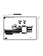
Page 24: ...3 X Z B 3 2 1 6 3 0 1 2 V 6 1 u 0 1 I151 I150 5VN_V I117 I112 I113 4124 R 0 3 3 8 3 1 3 p 0 0 1 5 1 1 2 GND 150R 3127 5VN_V p 0 0 1 1 5 1 2 1 4 1 I I143 0 4 1 I 4111 GND 4113 4 1 1 2 0 u 1 p 0 0 1 3 1 1 2 4118 4117 GND 7116 BC847BW 5 4 6 GND 3 1 2 MSD 244V 88 NI FE LF RED_BLACK 1131 2 MSD 244V 88 NI FE LF GREEN_BLUE 1131 1 I146 4 1 1 6 2 1 C 4 8 3 X Z B 1u0 2121 6 1 1 2 p 0 0 1 5V_V n 0 0 1 4 0 1 ...

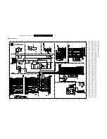
Page 25: ... 22u 16V p 0 0 1 4 0 2 2 3V3_A 3V3_A I206 u 0 0 1 1 1 2 5 I205 2 3 1 5 4 7214 74LVC1G125GW 5V 12V K 0 0 1 2 0 2 3 p 3 3 2 6 2 2 6 3V 2242 47u n 0 0 1 6 4 2 2 3243 680R 1u0 2208 3235 2212 1u0 22R 100K 3225 100n 2256 GND 1 1 2 3 0 K 1 22n 2259 5VN_A 5VN 1 3 2 1K0 3223 3 4 2 2 7210 BC817 25W n 0 0 1 22R 3237 3V3_A 3249 I230 100R 5VN_A I228 GND 2235 47u 6 3V 13 22R 3231 4 10 2 1 1 1 7 1 12 5 0 2 7206 ...

Page 26: ...30 SC2_IN_L 37 SC2_IN_R 38 STBYQ 11 N E T S E T 4 P T 7 1 F E R V 9 2 2 F E R V 5 2 3 2 4 2 8 2 2 3 RESETQ 22 SC1_IN_L 40 SC1_IN_R 41 SC1_OUT_L 31 SC1_OUT_R I2C_CL 12 I2C_DA 13 I2S_CL 14 I2S_DA_IN1 17 I2S_DA_IN2 21 I2S_DA_OUT 16 I2S_WS 15 MONO_IN 43 1 M _ L P A C 4 3 DACM_L 27 DACM_R 26 S S V D 0 2 DVSUP 19 0 O I _ R T C _ D 9 1 O I _ R T C _ D 8 AGNDC 36 S S V H A 5 3 P U S V H A 3 3 ANA_IN 2 ANA...

Page 27: ... 7 4 3 1 4 3 7 K 4 2 4 4 3 1 2 3 4 I410 B4B EH A 1405 GND u 0 3 3 1 1 4 2 3 1 4 6 6 1 3 S A B 3454 1K0 I423 3V3 GND V 2 1 6411 BZX384 C6V8 10K 3429 BC847BW 7424 GND GND 1K0 3453 V 0 5 u 0 1 8 1 4 2 I405 T 125mA 1414 2 2 4 6 2 V 8 C 4 8 3 X Z B 3431 100R 6 3 4 I426 7414 SI3443DV 1 2 5 0 R 1 5 4 4 3 2 V 8 C 4 8 3 X Z B 2 1 4 6 I432 GND I422 33VSTBY I424 8 K 1 4 3 4 3 K 0 2 2 GND 12VH 2 2 4 3 7415 BC...

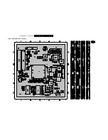
Page 28: ...EN 28 3139 785 33120 7 Circuit Diagrams and PWB Layouts Layout Analog Main Part Top View 3380_APAC_TOPLAYR pdf 2006 05 25 ...

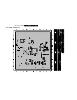
Page 29: ...EN 29 3139 785 33120 7 Circuit Diagrams and PWB Layouts Layout Analog Main Part Bottom View Analog Bottom 3139 243 33342_sh132_a3 eps 2007 09 26 ...

Page 30: ...11 10n 2117 10K 3118 100n 2119 6109 BAS316 2110 2n2 1216 EVQ11L05R 3122 10R 5102 GND 1207 EVQ11L05R GND 50V 22u 2107 3107 470R F116 2K7 3132 F135 6111 BAS316 6116 3131 2K7 BAS316 F112 GND 6102 BAS316 2118 22u 50V 11 1 27 28 52 51 50 2 3 42 43 45 46 47 4 4 8 4 12 5 4 8 17 18 19 20 21 22 23 7 49 13 41 32 33 34 35 16 36 37 38 39 40 9 10 14 15 24 25 26 29 30 31 6 BAS316 6114 BAS316 6213 10K 3108 2n2 2...

Page 31: ...1 2 4 2204 100n 3204 600R 1 F212 2 3 4 5 6 F213 1501 1 1402 1 2 3 4 3 4 C 5 6 5401 042 101 92 YKF51 5362 1202 1 2 Y 75R 3201 F205 GND F206 GND F211 GND GND GND GND F208 600R 3205 2205 470p F203 100p 2209 GND GND F207 GND GND GND F209 F200 75R 3206 YELLOW LPV8529 0100F 1301 1 1 2 75R GND 3202 GND GND F210 GND GND GND 2400 GND GND 1n0 470p 2206 F204 2 3 4 1502 CSS5004 7A01E 1 100p 2208 2207 100p F20...

Page 32: ... Diagrams and PWB Layouts Layout Front Panel Top Copper Pattern SMD Components Layout Front Panel Bottom Copper Pattern Components Front Top 3139 243 33415_sh132_a3 eps 2007 09 27 Front Bottom 3139 243 33415_sh132_a3 eps 2007 10 08 ...

Page 33: ...1 1303 C3 2301 C1 2 3 4 A C B 4 1 F300 C2 6301 C2 D E A B C D I300 EVQ11L05R F301 F300 1303 2n2 GND 2301 BZX384 C6V8 6300 1 2 6301 BZX384 C6V8 1302 WH02D 1 3139 243 33405_sh130 3_a4 eps 2007 09 27 Front Standby Top 3139 243 33395_sh132_a4 eps 2007 09 27 Layout Standby Bottom View Front Standby Bot 3139 243 33395_sh132_a4 eps 2007 09 27 ...

Page 34: ... C8 B10 B11 A11 C11 C12 B12 A12 B13 A13 B15 C18 A19 D18 C10 A16 A10 C13 C14 B14 A14 A15 C15 A20 A21 C20 B16 C16 D16 B17 C17 D17 B18 B19 B23 B22 A22 B21 C25 B26 C24 A26 B20 A3 A4 B4 A5 A6 B5 A7 A8 A17 A18 C19 6 7101 3 DMN 8652 DAC VIDEO Φ 3182 3 22R 3 BLM18P 5135 3174 3 47R 3 6 3165 22R T119 T117 T118 u 0 2 2 3198 1K0 1 8 V 6 1 1 8 1 2 47R 3173 1 n 0 0 1 2 4 1 2 5121 BLM31 n 0 0 1 3 4 1 2 K 0 1 6 1...

Page 35: ...2264 4 5 47R 3265 4 3253 4 4 5 47R 2292 100n 2 7 47R 3281 2 2 7 47R 3261 2 1 8 47R 3271 1 100R 3237 4 100R 3237 3 3237 2 100R 100R 3237 1 100R 3235 4 100R 3235 3 100R 3235 2 100n 2236 100R 3245 4 100R 3245 3 100R 3239 1 100R 3239 2 100R 3239 3 100R 3239 4 3235 1 100R 100R 3233 1 100R 3233 2 100R 3233 3 100R 3233 4 100R 3231 4 100R 3231 3 47R 3251 3 3 6 2267 100n 100n 2256 2255 100n 3277 3 47R 3 6 ...

Page 36: ...5 4361 E5 IEEE1394 Link Physical LNK T313 E7 T314 E7 T315 F6 T316 F6 T317 C6 T321 F6 T351 E6 T352 E6 5301 C6 7301 D6 T301 E7 T302 E7 T303 E7 T304 E7 T305 E7 T306 E7 T307 E7 3304 10K 5301 BLM18P T311 2 4 3 3 n 0 0 1 1 2 3 2 1 R 6 5 T307 T321 T312 T305 27 31 42 43 1K0 3301 33 34 37 23 24 1 22 30 29 28 9 4 19 13 48 16 17 18 12 1 4 0 4 10 11 4 1 6 4 7 4 1 2 4 4 5 4 38 39 5 3 20 2 3 15 4 5 6 7 8 9 1 PO...

Page 37: ...1 T402 4482 1 R 5 7 5 7 4 3 270R 3423 5431 BLM18P 5403 600R T461 4 3 4 2 T435 n 0 0 1 n 0 0 1 5 3 4 2 1 2 7 4 3 R 5 7 T422 6 0 M 1 1 6 4 3 3492 3 22R 3 n 0 0 1 2 1 4 2 n 0 0 1 3 1 4 2 n 0 0 1 2 0 4 2 4481 T433 T412 T411 T431 T408 3492 1 1 8 T409 T405 22R 4486 T400 3484 22R n 0 0 1 6 2 4 2 3430 270R 4484 p 0 0 1 8 8 4 2 7 2 4 2 p 0 0 1 4 8 4 2 3492 2 2 7 n 0 0 1 22R p 0 0 1 5 8 4 2 100n 2474 3457 2...

Page 38: ...81 T697 33R 3584 4 4 5 33R 3588 3 T596 T613 T522 T681 T678 3565 22R 22R 3541 p 2 2 3 4 5 2 T701 33R 3578 T588 T595 T559 7511 BC857B T504 T572 3552 22R T695 5525 0 3 5 3 0 K 1 10u 22R 3559 5 1 5 2 V 5 3 u 2 2 n 0 0 1 7 0 5 2 5 6 7 8 9 4 2 S S 1 2 5 6 33 34 35 36 37 38 39 4 40 22 23 24 25 26 27 28 29 3 30 31 32 14 15 16 17 18 19 2 20 21 1 1734160 4 1571 1 10 11 12 13 T548 3545 T502 22R 22R 3558 2 7 ...

Page 39: ...EN 39 3139 785 33120 7 Circuit Diagrams and PWB Layouts Layout Digital Main Part Top View Digital Top 3139 243 34464_sh132_a3 eps 2007 09 27 ...

Page 40: ...EN 40 3139 785 33120 7 Circuit Diagrams and PWB Layouts Layout Digital Main Part Bottom View Digital Bottom 3139 243 34464_sh132_a3 eps 2007 09 27 ...

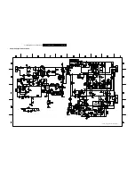
Page 41: ...EN 41 3139 785 33120 7 Circuit Diagrams and PWB Layouts Power Supply Unit Schematic AC7012_Sch_Rev 4 eps 2007 09 27 ...

Page 42: ...EN 42 3139 785 33120 7 Circuit Diagrams and PWB Layouts Power Supply Unit Layout The PSU Layout is not available ...

Page 43: ...SEL I2C_CL I2C_DA 13 12 10 43 37 38 40 41 39 21 17 2 3 18 ADR_CL I2S_WS XTAL_IN I2S_CL XTAL_OUT 14 15 5 6 AVSS 44 AHVSS AGNDC DVSS VREF1 VREF2 VREFTOP RESETQ STANDBYQ TESTEN TP 7 4 11 22 42 25 29 20 36 35 CAPL_M 34 DVSUP AVSUP AHVSUP 33 19 1 N C 23 24 28 32 N C N C N C De Modulator Pre processing Source select Pre processing ADC ADC Prescale SCART DSP input select Loud speaker sound proeessing Lou...

Page 44: ...17 16 15 14 13 12 1 2 3 4 5 6 7 8 9 10 11 33 32 31 30 29 28 27 26 25 24 23 Figure 8 9 IC7206 192KHz Stereo DAC with 2vrms line out BLOCK DIAGRAM PCM Serial Interface Interpolation Filter with Volume Control Internal Voltage Reference External Mute Control DAC Serial Audio Input Left and Right Mute Controls 2 Vrms Line Level Right Channel Output 2 Vrms Line Level Left Channel Output Reset 1 8 V to ...

Page 45: ...17 High Voltage Analog Power Input Positive power supply for the analog section VL 20 Serial Audio Interface Power Input Positive power for the serial audio interface BMUTEC AMUTEC 14 19 Mute Control Output Control signal for optional mute circuit AOUTB AOUTA 15 18 Analog Outputs Output The full scale analog line output level is specified in the Analog Characteris tics table Control Port Definitio...

Page 46: ... channel input Vref 2 reference voltage VINR 3 right channel input VRN 4 negative reference voltage VRP 5 positive reference voltage SFOR 6 data format selection input PWON 7 power control input SYSCLK 8 system clock 256 384 512 or 768fs VDDD 9 digital supply voltage VSSD 10 digital ground BCK 11 bit clock input output WS 12 word select input output DATAO 13 data output MSSEL 14 master slave selec...

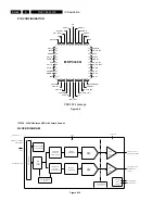
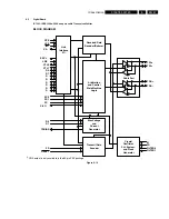
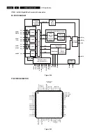
Page 47: ...rface I O Arbitration and Control State Machine Logic Bias Voltage and Current Generator Transmit Data Encoder Cable Port Crystal Oscillator PLL System and Clock Generator TPA CPS TPA TPB TPB XI XO FILTER0 FILTER1 LPS ISO C A S SCL LRE CTL0 CTL1 D0 D1 D D D D D D PC0 PC1 PC C L O R0 R1 TPBIAS PD RESET CNA output is only available in the 64 pin PAP package Figure 8 12 ...

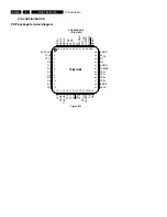
Page 48: ...VDD 36 35 34 33 32 31 30 29 28 27 26 25 16 1 2 3 4 5 6 7 8 9 10 11 12 SYSCLK CTL0 CTL1 D0 D1 D2 D3 D4 D5 D6 D7 PD 17 18 19 20 47 46 45 44 43 48 42 40 39 38 41 21 22 23 24 37 13 PHP PACKAGE TOP VIEW TSB41AB1 PLLGND PLLV FILTER1 FILTER0 LREQ DGND DGND DV TESTM SE SM C LKON PC1 PC2 ISO CPS DV RESET XO XI DGND LPS PC0 DD DV DD DD DD Figure 8 13 ...

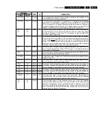
Page 49: ...w except during hardware reset when it is high impedance The link on output is activated if the LLC is inactive LPS inactive or the LCtrl bit cleared and when a the PHY receives a link on PHY packet addressed to this node or b the PEI port event interrupt register bit is 1 or c any of the CTOI configuration time out interrupt CPSI cable power status interrupt or STOI state time out interrupt regis...

Page 50: ...wered see Figure 9 A pulsed signal should be used when an isolation barrier exists between the LLC and PHY See Figure 10 The LPS input is considered inactive if it is sampled low by the PHY for more than 2 6 µs 128 SYSCLK cycles and is considered active otherwise that is asserted steady high or an oscillating signal with a low time less than 2 6 µs The LPS input must be high for at least 21 ns to ...

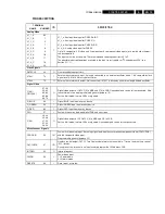
Page 51: ... input is used in manufacturing test of the TSB41AB1 For normal use this terminal should be tied to GND 1 CMOS O System clock output Provides a 49 152 MHz clock signal synchronized with data transfers to the LLC 22 CMOS I Test control input This input is used in manufacturing test of the TSB41AB1 For normal use this terminal should be tied to VDD 30 Cable I O Twisted pair cable A differential sign...

Page 52: ...NFIGURATION 22 23 C_6 GPIO RED C_7 GPIO GREEN C_8 GPIO BLUE C_9 GPIO FSO DGND DVDD Y_0 Y_1 Y_2 Y_3 Y_4 IOGND IOVDD Y_5 Y_6 Y_7 Y_8 Y_9 DGND DVDD 60 59 58 57 56 55 54 53 52 51 50 49 48 47 46 45 44 43 42 41 24 1 2 3 4 5 6 7 8 9 10 11 12 13 14 15 16 17 18 19 20 VI_1_B VI_1_C CH1_A33GND CH1_A33VDD CH2_A33VDD CH2_A33GND VI_2_A VI_2_B VI_2_C CH2_A18GND CH2_A18VDD A18VDD_REF A18GND_REF CH3_A18VDD CH3_A18...

Page 53: ...single ended oscillator Digital Video C 9 0 GPIO 9 0 57 58 59 60 63 64 65 66 69 70 O Digital video output of CbCr C 9 is MSB and C 0 is LSB Unused outputs can be left unconnected Also these terminals can be programmable general purpose I O For the 8 bit mode the two LSBs are ignored D_BLUE 58 I Digital BLUE input from overlay device D_GREEN 59 I Digital GREEN input from overlay device D_RED 60 I D...

Page 54: ...VDD CH4_A33VDD 4 5 20 21 I Analog power Connect to 3 3 V DGND 27 32 42 56 68 I Digital return DVDD 31 41 55 67 I Digital power Connect to 1 8 V IOGND 39 49 62 I Digital power return IOVDD 38 48 61 I Digital power Connect to 3 3 V or less for reduced noise LL_A18GND 77 I Analog power return LL_A18VDD 76 I Analog power Connect to 1 8 V Sync Signals HS CS GPIO 72 I O Horizontal sync output or digital...

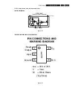
Page 55: ...lay BLOCK DIAGRAM NCP303LSNxxT1 Open Drain Output Configuration Vref 2 Input 3 Gnd 5 CD RD 1 Reset Output Figure 8 18 PIN DESCRIPTION AND CONFIGURATION PIN CONNECTIONS AND MARKING DIAGRAM 1 3 N C Reset Output 2 Input Ground 4 CD 5 xxxYW Top View xxx 302 or 303 Y Year W Work Week Figure 8 19 ...

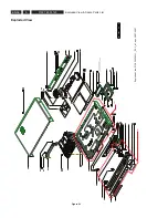
Page 56: ...4 2x 252 2x 253 240 264 3x 263 4x 256 3x 1004 184 260 265 273 2x 230 187 1002 258 3x 257 4x 1006 183 186 251 8x 1003 125 124 126 123 250 181 101 129 128 ENVIRONMENTAL REQUIREMENT NO BANNED SUBSTANCES ACC TO UAT 0480 100 P002 P001 270 for DVDR3455H DVDR3465H 274 for DVDR3450H DVDR3460H DVDR3452H Exploded View 3139 249 36541_110 1_a1 eps 2007 09 27 9 Exploded View Spare Parts List ...

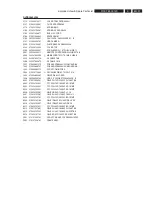
Page 57: ...BAS DVDR3455H ANA BOARD NA 1003 313924889112 FRONT COMBI PCBA 1004 313924712864 PSU 06H85 WR AC7012X LF PIE 1005 313924800561 DRIVE D6 8 CLOSED 1006 282206200152 HDD 3 5 250GB ST3250820ACE B 8002 313911028301 CBLE PH 12P 220 12P PH 26ST BK 8003 313924102541 FFC FOIL 18P 180 18P AD 1MMP 8004 313924102551 FFC FOIL 19P 180 19P AD 1MMP 8005 313924102531 FFC FOIL 24P 140 24P AD 1MMP 8006 313924102061 C...

Reviews: