EN 42
3139 785 30981
7.
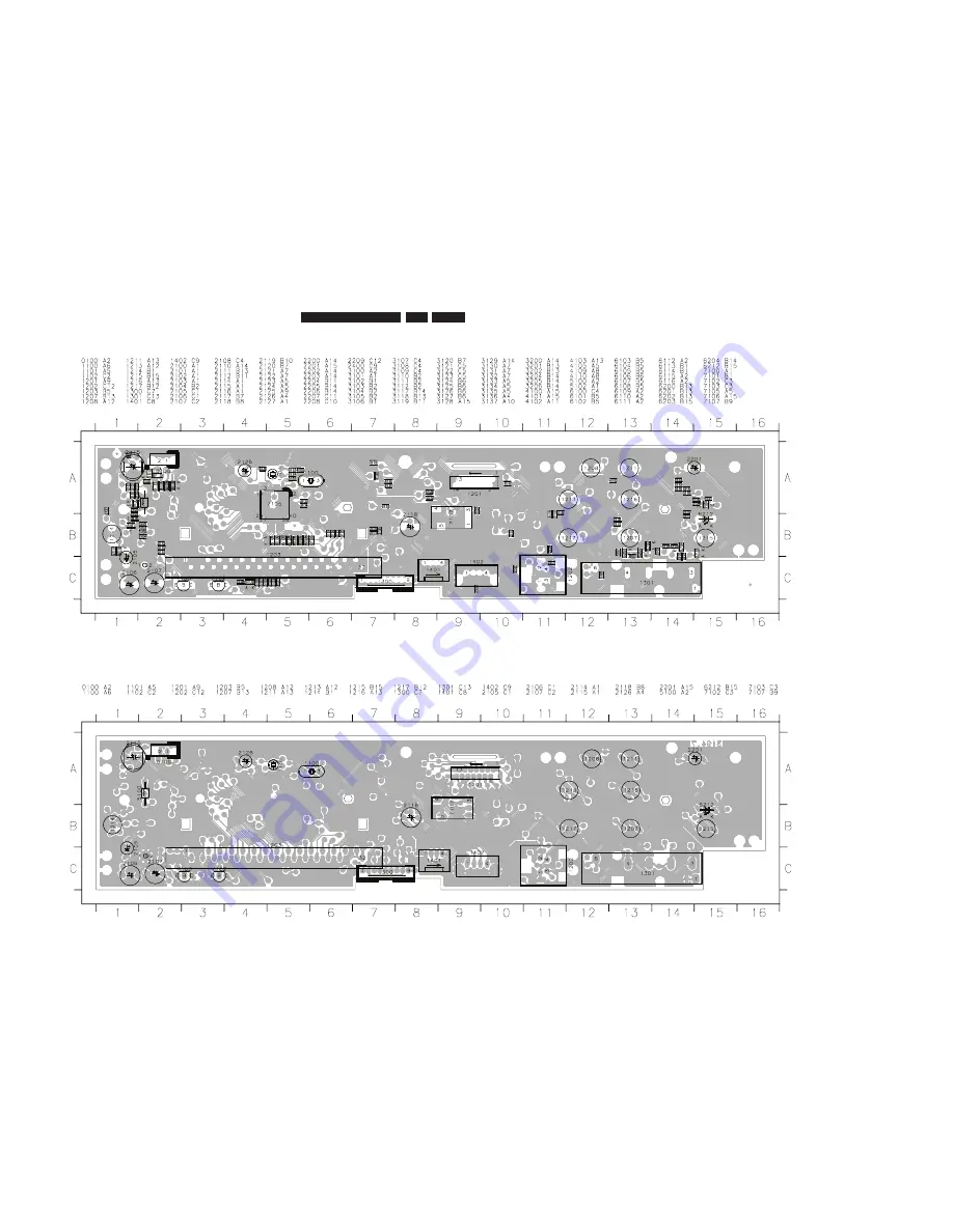
Circuit Diagrams and PWB Layouts
Layout: Front Panel (Top Copper Pattern) - SMD + Components
Layout: Front Panel (Bottom Copper Pattern) - Components
FrontPanel_Topview_31947_3355.eps 2005-04-01
FrontPanel_Bottomview_31947_3355.eps 2005-04-01


