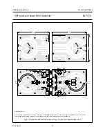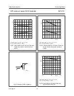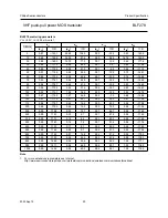
background image

2003 Sep 19

9

Philips Semiconductors

Product Specification

VHF push-pull power MOS transistor

BLF278

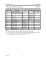
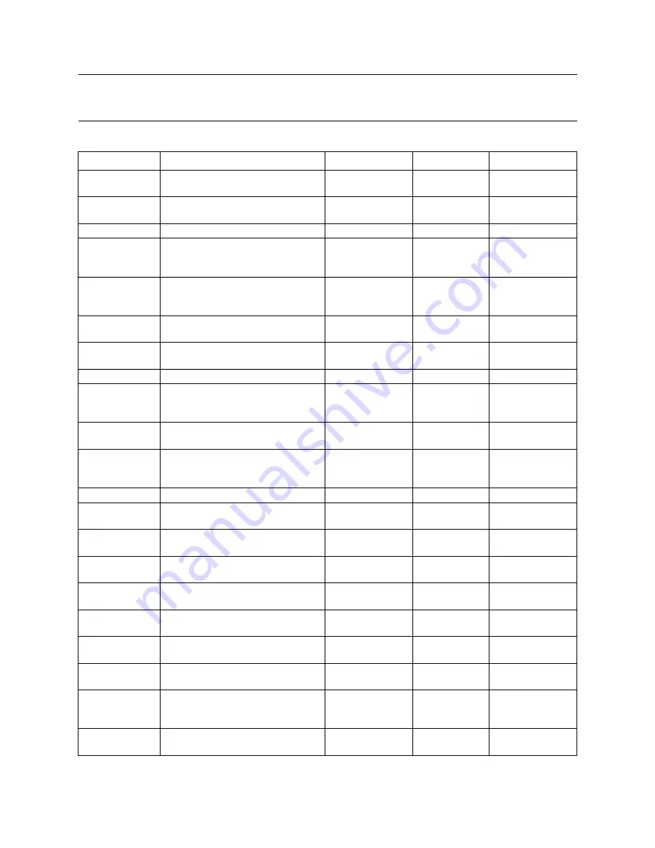
List of components (see Figs 12 and 13).

COMPONENT

DESCRIPTION

VALUE

DIMENSIONS

CATALOGUE NO.

C1, C2, C33, C34 multilayer ceramic chip capacitor;

note 1

22 pF, 500 V

C3, C4

multilayer ceramic chip capacitor;
note 1

100 pF + 68 pF
in parallel, 500 V

C5, C6, C28

film dielectric trimmer

5 to 60 pF

2222 809 08003

C7

multilayer ceramic chip capacitor;
note 1

2

×

100 pF +

1

×

120 pF in

parallel, 500 V

C8, C11, C12,
C15, C16, C19,
C36

multilayer ceramic chip capacitor

100 nF, 500 V

2222 852 47104

C9, C10, C13,
C14, C20, C25

multilayer ceramic chip capacitor;
note 1

1 nF, 500 V

C17, C18, C22,
C23

multilayer ceramic chip capacitor;
note 1

470 pF, 500 V

C21, C24, C35

electrolytic capacitor

10

µ

F, 63 V

C26

multilayer ceramic chip capacitor;
note 1

2

×

15 pF +

1

×

18 pF in

parallel, 500 V

C27

multilayer ceramic chip capacitor;
note 1

3

×

15 pF in

parallel, 500 V

C29

multilayer ceramic chip capacitor;
note 1

2

×

18 pF +

1

×

15 pF in

parallel, 500 V

C30

film dielectric trimmer

2 to 18 pF

2222 809 09006

C31, C32

multilayer ceramic chip capacitor;
note 1

3

×

43 pF in

parallel, 500 V

L1, L2

stripline; note 2

43

length 57.5 mm
width 6 mm

L3, L4

stripline; note 2

43

length 29.5 mm
width 6 mm

L5, L6

stripline; note 2

43

length 14 mm
width 6 mm

L7, L8

stripline; note 2

43

length 6 mm
width 6 mm

L9, L10

stripline; note 2

43

length 17.5 mm
width 6 mm

L11, L16

2

×

grade 3B Ferroxcube wideband

HF chokes in parallel

4312 020 36642

L12, L15

4 turns enamelled 2 mm copper wire

85 nH

length 13.5 mm
int. dia. 10 mm
leads 2

×

7 mm

L13, L14

stripline; note 2

43

length 19.5 mm
width 6 mm

Summary of Contents for BLF278 -

Page 1: ...DATA SHEET Product Specification Supersedes data of 1996 Oct 21 2003 Sep 19 DISCRETE SEMICONDUCTORS BLF278 VHF push pull power MOS transistor M3D091 ...

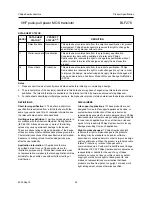
Page 2: ...efer to Philips specs SNW EQ 608 SNW FQ 302A and SNW FQ 302B PIN DESCRIPTION 1 drain 1 2 drain 2 3 gate 1 4 gate 2 5 source Fig 1 Simplified outline and symbol 1 2 3 4 MAM098 Top view 5 5 d g s d g QUICK REFERENCE DATA RF performance at Th 25 C in a push pull common source test circuit MODE OF OPERATION f MHz VDS V PL W Gp dB ηD CW class B 108 50 300 20 60 CW class C 108 50 300 typ 18 typ 80 CW cl...

Page 3: ...ion temperature 200 C SYMBOL PARAMETER CONDITIONS VALUE UNIT Rth j mb thermal resistance from junction to mounting base total device both sections equally loaded max 0 35 K W Rth mb h thermal resistance from mounting base to heatsink total device both sections equally loaded max 0 15 K W Fig 2 DC SOAR Total device both sections equally loaded 1 Current is this area may be limited by RDSon 2 Tmb 25...

Page 4: ...sconductance VDS 10 V ID 5 A 4 5 6 2 S gfs1 gfs2 forward transconductance ratio of both sections VDS 10 V ID 5 A 0 9 1 1 RDSon drain source on state resistance VGS 10 V ID 5 A 0 2 0 3 Ω IDSX drain cut off current VGS 10 V VDS 10 V 25 A Cis input capacitance VGS 0 VDS 50 V f 1 MHz 480 pF Cos output capacitance VGS 0 VDS 50 V f 1 MHz 190 pF Crs feedback capacitance VGS 0 VDS 50 V f 1 MHz 14 pF Cd f ...

Page 5: ...s a function of gate source voltage typical values per section VDS 10 V Tj 25 C handbook halfpage 0 30 20 10 0 5 ID A 10 VGS V 15 MGE622 Fig 6 Drain source on state resistance as a function of junction temperature typical values per section VGS 10 V ID 5 A handbook halfpage 0 50 100 150 400 0 200 100 300 MGE621 RDSon mΩ Tj C Fig 7 Input and output capacitance as functions of drain source voltage t...

Page 6: ...mance in CW operation in a common source push pull test circuit Th 25 C Rth mb h 0 15 K W unless otherwise specified RGS 4 Ω per section optimum load impedance per section 3 2 j4 3 Ω VDS 50 V Ruggedness in class B operation The BLF278 is capable of withstanding a load mismatch corresponding to VSWR 7 1 through all phases under the following conditions VDS 50 V f 108 MHz at rated load power MODE OF...

Page 7: ...00 600 MGE682 PL W Gp dB 1 2 Fig 10 Efficiency as a function of load power typical values Class B operation VDS 50 V IDQ 2 0 1 A f 108 MHz ZL 3 2 j4 3 Ω per section RGS 4 Ω per section 1 Th 25 C 2 Th 70 C handbook halfpage 0 200 400 PL W 600 80 60 ηD 20 0 40 MGE683 1 1 2 2 Fig 11 Load power as a function of input power typical values Class B operation VDS 50 V IDQ 2 0 1 A f 108 MHz ZL 3 2 j4 3 Ω p...

Page 8: ... text is here inThis text is here in white to force landscape pages to be rotated correctly when browsing through the pdf in the Acrobat reader white to force landscape pages to be Fig 12 Class B test circuit at f 108 MHz handbook full pagewidth MGE688 R11 IC1 C36 C37 C11 C35 L14 L18 L20 R5 C14 C15 C10 R6 R7 R2 R3 R4 L1 T1 C5 C4 C3 R1 C1 C2 C6 C7 C27 C28 C26 C29 C30 C33 C31 L21 L22 L23 L19 L17 L13...

Page 9: ... pF 500 V C21 C24 C35 electrolytic capacitor 10 µF 63 V C26 multilayer ceramic chip capacitor note 1 2 15 pF 1 18 pF in parallel 500 V C27 multilayer ceramic chip capacitor note 1 3 15 pF in parallel 500 V C29 multilayer ceramic chip capacitor note 1 2 18 pF 1 15 pF in parallel 500 V C30 film dielectric trimmer 2 to 18 pF 2222 809 09006 C31 C32 multilayer ceramic chip capacitor note 1 3 43 pF in p...

Page 10: ...4 5 mm width 6 mm L19 L20 stripline note 2 43 Ω length 66 mm width 6 mm L21 L23 stripline note 2 50 Ω length 160 mm width 4 8 mm L22 semi rigid cable note 3 50 Ω ext dia 3 6 mm outer conductor length 160 mm R1 metal film resistor 10 Ω 0 4 W R2 R7 10 turn potentiometer 50 kΩ R3 R6 metal film resistor 3 12 1 Ω in parallel 0 4 W R4 R5 metal film resistor 10 Ω 0 4 W R8 R9 metal film resistor 10 Ω 5 1 ...

Page 11: ...onnections are made by means of copper straps for a direct contact between upper and lower sheets Dimensions in mm handbook full pagewidth 130 150 100 strap strap strap strap strap strap strap strap MBC438 R1 C3 C2 C1 C4 L1 L2 C6 R11 C36 L3 L4 IC1 VDD1 R2 and R7 C8 C11 C7 L5 L6 L7 L8 C9 C13 R3 C12 slider R2 R4 slider R7 C15 R6 R5 C10 C14 C23 C24 C25 C19 C18 VDD2 L11 R8 L11 C22 C21 C20 C16 C17 VDD1...

Page 12: ...ri xi 1 2 0 MGE685 Fig 15 Load impedance as a function of frequency series components typical values per section Class B operation VDS 50 V IDQ 2 0 1 A RGS 4 Ω per section PL 300 W handbook halfpage 25 75 125 f MHz 175 8 6 ZL Ω XL RL 2 0 4 MGE686 Fig 16 Definition of MOS impedance handbook halfpage MBA379 Zi ZL Fig 17 Power gain as a function of frequency typical values per section Class B operati...

Page 13: ... 15 K W unless otherwise specified RGS 2 8 Ω per section optimum load impedance per section 0 74 j2 Ω VDS 50 V Ruggedness in class AB operation The BLF278 is capable of withstanding a load mismatch corresponding to VSWR 7 1 through all phases under the following conditions VDS 50 V f 225 MHz at rated output power MODE OF OPERATION f MHz VDS V IDQ A PL W Gp dB ηD CW class AB 225 50 2 0 5 250 14 typ...

Page 14: ...0 0 10 MGE614 Gp dB PL W 2 1 Fig 19 Efficiency as a function of load power typical values Class AB operation VDS 50 V IDQ 2 0 5 A f 225 MHz ZL 0 74 j2 Ω per section RGS 2 8 Ω per section 1 Th 25 C 2 Th 70 C handbook halfpage 0 60 40 ηD 20 0 100 200 PL W 300 MGE612 2 1 Fig 20 Load power as a function of input power typical values Class AB operation VDS 50 V IDQ 2 0 5 A f 225 MHz ZL 0 74 j2 Ω per se...

Page 15: ...xt is here inThis text is here in white to force landscape pages to be rotated correctly when browsing through the pdf in the Acrobat reader white to force landscape pages to be Fig 21 Class AB test circuit at f 225 MHz handbook full pagewidth MGE617 L13 C17 C18 C19 R9 R11 IC1 C38 C37 C36 C35 L17 C26 C27 C25 L19 L21 R5 C12 C13 C9 R6 R7 L16 C22 C14 C23 C24 L14 R8 R2 R3 R4 L4 L1 C5 C4 C3 R1 C1 C2 C6...

Page 16: ...0 µF 63 V C20 multilayer ceramic chip capacitor note 1 3 33 pF in parallel 500 V C21 film dielectric trimmer 2 to 9 pF 2222 809 09005 C22 C27 C37 C38 multilayer ceramic chip capacitor note 1 1 nF 500 V C23 C26 C35 electrolytic capacitor 10 µF 63 V C24 C25 multilayer ceramic chip capacitor note 1 2 470 pF in parallel 500 V C28 multilayer ceramic chip capacitor note 1 2 10 pF 1 18 pF in parallel 500...

Page 17: ...L24 respectively L14 L17 2 grade 3B Ferroxcube wideband HF chokes in parallel 4312 020 36642 L15 L16 13 4 turns enamelled 2 mm copper wire 40 nH int dia 10 mm leads 2 7 mm space 1 mm L18 L19 stripline note 2 43 Ω length 13 mm width 6 mm L20 L21 stripline note 2 43 Ω length 29 5 mm width 6 mm R1 metal film resistor 10 Ω 0 4 W R2 R7 10 turns potentiometer 50 kΩ R3 R6 metal film resistor 1 kΩ 0 4 W R...

Page 18: ...e by means of copper straps for a direct contact between upper and lower sheets Dimensions in mm handbook full pagewidth MBC436 119 130 100 Hollow rivets Hollow rivets strap strap strap strap strap strap strap strap R11 C38 C35 C37 C36 C16 IC1 L2 L1 R1 C1 C2 C3 C4 C5 L4 L5 C6 slider R2 slider R7 C13 R6 C12 C17 L10 L11 R4 R5 L8 L6 L7 L9 VDD1 C10 R3 C11 C8 to R2 R7 VDD1 VDD2 C9 C7 L17 R9 L17 C18 C25...

Page 19: ...611 ri zi Ω xi f MHz Fig 24 Load impedance as a function of frequency series components typical values per section Class AB operation VDS 50 V IDQ 2 0 5 A RGS 2 8 Ω per section PL 250 W handbook halfpage 150 250 200 f MHz 3 2 1 0 MGE625 XL RL ZL Ω Fig 25 Definition of MOS impedance handbook halfpage MBA379 Zi ZL Fig 26 Power gain as a function of frequency typical values per section Class AB opera...

Page 20: ...70 0 93 174 1 3 26 44 9 0 01 18 3 0 78 166 5 80 0 94 174 7 2 66 41 0 0 01 19 8 0 80 166 5 90 0 95 175 2 2 22 37 5 0 00 19 7 0 83 166 7 100 0 95 175 7 1 88 34 0 0 00 18 0 0 85 167 4 125 0 97 176 9 1 27 26 8 0 00 1 9 0 88 169 4 150 0 97 177 9 0 91 22 7 0 00 35 3 0 91 170 0 175 0 98 178 7 0 69 19 5 0 00 65 3 0 94 170 8 200 0 98 179 5 0 54 16 0 0 00 78 0 0 95 172 4 250 0 99 179 2 0 35 12 1 0 01 86 7 0...

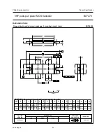
Page 21: ... w1 A B M M M B M w3 M M w2 C UNIT A mm D b 5 85 5 58 0 16 0 10 22 17 21 46 11 05 10 29 10 03 21 08 19 56 9 91 9 65 5 77 5 00 c e U2 0 25 0 25 0 51 w3 27 94 q w2 w1 F 1 78 1 52 U1 34 17 33 90 H1 17 02 16 51 p 3 28 3 02 Q 2 85 2 59 E E1 D1 10 27 10 05 inches 0 230 0 220 0 006 0 004 0 873 0 845 21 98 21 71 0 865 0 855 0 435 0 405 0 396 0 830 0 770 0 390 0 380 0 227 0 197 0 010 0 010 0 020 1 100 0 07...

Page 22: ...tion Limiting values given are in accordance with the Absolute Maximum Rating System IEC 60134 Stress above one or more of the limiting values may cause permanent damage to the device These are stress ratings only and operation of the device at these or at any other conditions above those given in the Characteristics sections of the specification is not implied Exposure to limiting values for exte...

Page 23: ...bility will be accepted by the publisher for any consequence of its use Publication thereof does not convey nor imply any license under patent or other industrial or intellectual property rights Philips Semiconductors a worldwide company Contact information For additional information please visit http www semiconductors philips com Fax 31 40 27 24825 For sales offices addresses send e mail to sale...

Reviews: