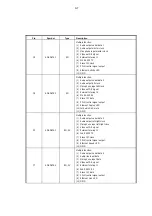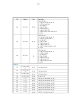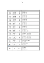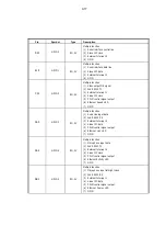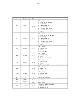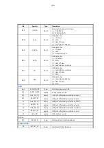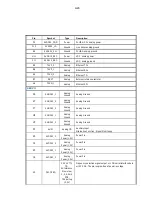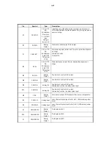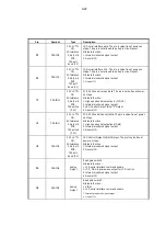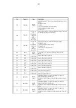
Pin Symbol Type
Description
L3
ʳ
FECMOD
3.3V LVTTL
I/O,
5V-tolerance,
Slow slew,
2, 4, 6, 8mA
PDR,
75K pull-
down (0V)
High frequency modulation mode selection signal output, or
LDD serial interface command enable. The pin is spike-free at
power-on stage.
P3
ʳ
FEDMO
Analog
Output
Disk motor control output. DAC output.
T1
ʳ
FEEJECT_
3.3V LVTTL
I/O,
5V-tolerance,
6 mA PDR,
75K pull-up
(3.3V)
Eject/stop key input, active low. The pin is spike-free at power-
on stage.
Alternate function :
General IO.
R1
ʳ
FEFG
3.3V LVTTL
I/O,
5V-tolerance,
6 mA PDR,
75K pull-up
(3.3V)
Motor Hall sensor input. The pin is spike-free at power-on
stage.
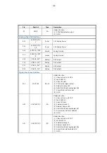
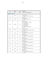
N1
ʳ
FEFMO
Analog
Output
Feed motor 1 control. DAC output.
N2
ʳ
FEFMO2
Analog
Output
Feed motor 2 control. DAC output.
N3
ʳ
FEFMO3
Analog I/O
Feed motor 3 control. DAC output.
Alternative Function : Auxiliary servo input
M3
ʳ
FEFMO4
Analog I/O
Feed motor 4 control. DAC output.
Alternative Function : Auxiliary servo input
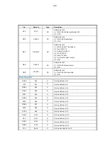
H4
ʳ
FOO
Analog
Output
Focus servo output. PDM output of focus servo compensator.
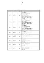
A3
ʳ
FPDOCD
Analog Input
Laser Power Monitor Input for CD APC / Differential negative
input
C4
ʳ
FPDODVD
Analog Input
Laser Power Monitor Input for DVD APC / Differential positive
input
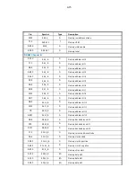
L2
ʳ
FEGAINSW1
Analog
Output
Read gain switch. 1
M2
ʳ
FEGAINSW2
Analog
Output
Read gain switch 2.
L1
ʳ
FEGAINSW3
Analog
Output
Read gain switch 3.
9-21
Summary of Contents for BDP2105
Page 11: ...4 3 5 SOURCE 1 2 TV 2 4 ...
Page 12: ...6 USB DVD VCD CD BD BD 3D DivX Plus HD MKV MP3 JPEG 2 3 4 1 1 2 3 2 5 ...
Page 40: ...7 6 7 6 Front Board Print layout bottom side for BDP2180 12 05 ...
Page 41: ...7 7 7 7 Front Board Print layout bottom side for BDP2180X 78 ...
Page 42: ...7 8 7 8 Front Board Print layout bottom side for BDP2180X 78 ...
Page 43: ...7 9 7 9 Power Board Print layout bottom side for BDP2180 12 05 X78 ...
Page 46: ...PIN ASSIGNMENT 9 2 ...

