background image

Service Modes, Error Codes, and Fault Finding

EN 15

TPM8.3A LA

5.

2011-Nov-11

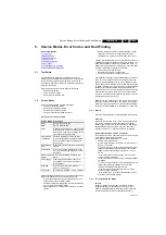
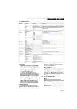
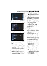
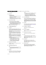
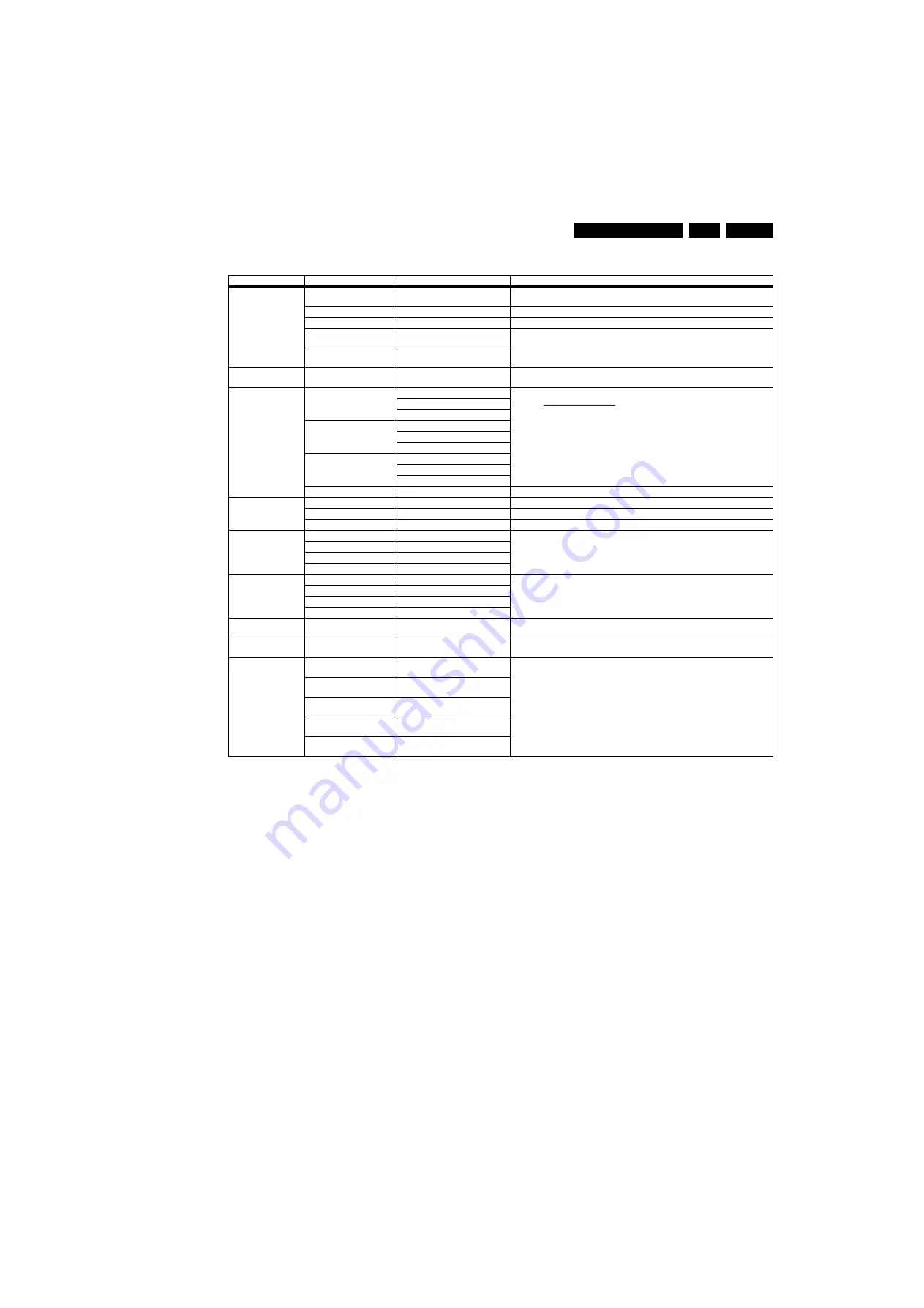
Table 5-2 SAM mode overview

How to Navigate

In the SAM menu, select menu items with the UP/DOWN 
keys on the remote control transmitter. The selected item 
will be indicated. When not all menu items fit on the screen, 
use the UP/DOWN keys to display the next/previous menu 
items.

With the “LEFT/RIGHT” keys, it is possible to:

(De) activate the selected menu item.

(De) activate the selected sub menu.

Change the value of the selected menu item.

When you press the MENU button twice while in top level 
SAM, the set will switch to the normal user menu (with the 
SAM mode still active in the background). To return to the 
SAM menu press the MENU button.

The “INFO [i+]” key from the user remote will toggle the 
OSD “on/off” with “SAM” OSD remaining always “on”.

Press the following key sequence on the remote control 
transmitter: “062596” directly followed by the MENU button 
to switch to SDM (do not allow the display to time out 
between entries while keying the sequence). Remarks: 
new RC will not have I+ button, but function still remain.

How to Store SAM Settings
To store the settings changed in SAM mode (except the 
RGB ALIGN settings), leave the top level SAM menu by using 
the POWER button on the remote control transmitter or the 

television set. The mentioned exceptions must be stored 
separately via the STORE button.

How to Exit SAM
Use one of the following methods:

Switch the set to STANDBY by pressing the mains button 
on the remote control transmitter or the television set.

Via a standard RC-transmitter, key in “00” sequence.

Note: When the TV is switched “off” by a power interrupt while 
in SAM, the TV will show up in “normal operation mode” as 
soon as the power is supplied again. The error buffer will not be 
cleared.

5.2.4

Customer Service Mode (CSM)

Purpose
The Customer Service Mode shows error codes and 
information on the operation settings of the TV. The call centre 
can instruct the customer (by telephone) to enter CSM in order 
to identify the status of the set.This helps the call centre to 
diagnose problems and failures in the TV set before making a 
service call.
The CSM is a read-only mode; therefore, modifications are not 
possible in this mode.

Main Menu

Sub-menu 1

Sub-menu 2

Description

System Information

Op Hour

This represents the life timer. The timer counts normal operation hours, but does not count 
Stand-by hours.

Main SW ID

e.g. “TPM82A 1.02”

See paragraph Software Identification, Version, and Cluster for the SW name definition.

ERR

e.g. “000 000 000 000 000”

Shows all errors detected since the last time the buffer was erased. Five errors possible.

OP1

e.g. “012 004 192 002 156 032 007 
026”

Option code is hard coded in SW, it cannot be edited in SAM mode. Only to show in 
SAM system information.

OP2

e.g. “056 023 000 106 064 000 000 
122”

Clear

Press [OK] to clean the Error 
Codes immediately

Erases the contents of the error buffer. Select this menu item and press the MENU RIGHT 
key on the remote control. The content of the error buffer is cleared.

RGB Align

Warm

R Gain

To align the White Tone. See 
paragrap

6.3 Software Alignments

 in the Alignments section for a detailed description

G Gain

B Gain

Normal

R Gain

G Gain

B Gain

Cool

R Gain

G Gain

B Gain

Store

Store the RGB value 

NVM editor

Address

Select and fill the NVM address

Value

Select and fill the NVM value

Store

Store the value in the address

Upload to USB

Copy Channel List to USB

To upload several settings from the TV to an USB stick

Copy NVM to USB

Copy Readable Info to USB

Copy Edid to USB

Download from USB

Copy Channel List from USB

To download several settings from the USB stick to the TV

Copy NVM from USB

Copy Readable Info from USB

Copy Edid from USB

Initialize NVM

Press [OK] to Initialize NVM 
immediately

To initialize a (corrupted) NVM. Be careful, this will erase all settings.

EDID Write Enable

Press [OK] to enable EDID 
writable immediately

Enable EDID writable

Service Data

Type Number

Press [OK] use key pad edit type 
number immediately

Use Key pad to edit several service data

Production Number

Press [OK] use key pad edit 
production number immediately

12NC SSB

Press [OK] use key pad edit SSB 
immediately

12NC PSU

Press [OK] use key pad edit PSU 
immediately

12NC Display

Press [OK] use key pad edit display 
immediately

Summary of Contents for 42PFL5606S/98

Page 1: ...Block Diagrams Wiring diagram 32 33 Wiring diagram 42 34 Block Diagram 35 10 Circuit Diagrams and PWB Layouts Drawing PWB A01 715G4867 PSU 32 36 AC PFC A01 36 39 40 Standby A02 37 39 40 Main Power A03 38 39 40 A01 715G4878 PSU 42 41 AC Side A01 41 47 48 Standby A02 42 47 48 DCM PFC A03 43 47 48 Second Power A04 44 47 48 Main Power A05 45 47 48 LED Driver A06 46 47 48 B 715G4611 SSB 49 PSU Inverter...

Page 2: ...ns for Use 2 3 Connections 2 4 Chassis Overview Notes Figures can deviate due to the different set executions Specifications are indicative subject to change 2 1 Technical Specifications For on line product support please use the links in Here is product information available as well as getting started user manuals frequently asked questions and software drivers Table 2 1 Described Model Numbers N...

Page 3: ...input from an antenna cable or satellite 5 Cinch Video CVBS In Audio In Ye Video CVBS 1 VPP 75 Ω jq Rd Audio R 0 5 VRMS 10 kΩ jq Wh Audio L 0 5 VRMS 10 kΩ jq 6 HDMI1 Digital Video Digital Audio In Figure 2 3 HDMI type A connector 1 D2 Data channel j 2 Shield Gnd H 3 D2 Data channel j 4 D1 Data channel j 5 Shield Gnd H 6 D1 Data channel j 7 D0 Data channel j 8 Shield Gnd H 9 D0 Data channel j 10 CL...

Page 4: ...1 Cinch Video YPbPr In Audio In Gn Video Y 1 VPP 75 Ω jq Bu Video Pb 0 7 VPP 75 Ω jq Rd Video Pr 0 7 VPP 75 Ω jq Wh Audio L 0 5 VRMS 10 kΩ jq Rd Audio R 0 5 VRMS 10 kΩ jq 12 Service UART 1 Ground Gnd H 2 UART_TX Transmit k 3 UART_RX Receive j 13 PC IN VGA Figure 2 4 VGA connector 1 Video Red 0 7 VPP 75 Ω j 2 Video Green 0 7 VPP 75 Ω j 3 Video Blue 0 7 VPP 75 Ω j 4 n c 5 Ground Gnd H 6 Ground Red G...

Page 5: ...475 25 MHz for PAL or 61 25 MHz for NTSC channel 3 Where necessary measure the waveforms and voltages with D and without E aerial signal Measure the voltages in the power supply section both in normal operation G and in stand by F These values are indicated by means of the appropriate symbols 3 3 2 Schematic Notes All resistor values are in ohms and the value multiplier is often used to indicate t...

Page 6: ...mes held in less regard Always respect voltages While some may not be dangerous in themselves they can cause unexpected reactions that are best avoided Before reaching into a powered TV set it is best to test the high voltage insulation It is easy to do and is a good service precaution 3 4 Abbreviation List 0 6 12 SCART switch control signal on A V board 0 loop through AUX to TV 6 play 16 9 format...

Page 7: ...rnational Telecommunication Union relating to radio communication ITU 656 a k a SDI is a digitized video format used for broadcast grade video Uncompressed digital component or digital composite signals can be used The SDI signal is self synchronizing uses 8 bit or 10 bit data words and has a maximum data rate of 270 Mbit s with a minimum bandwidth of 135 MHz iTV Institutional TeleVision TV sets f...

Page 8: ...ck I2C SCL F CLock Signal on Fast I2 C bus SD Standard Definition SDA Serial Data I2C SDA F DAta Signal on Fast I2 C bus SDI Serial Digital Interface see ITU 656 SDRAM Synchronous DRAM SECAM SEequence Couleur Avec Mémoire Colour system mainly used in France and East Europe Colour carriers 4 406250 MHz and 4 250000 MHz SIF Sound Intermediate Frequency SMPS Switched Mode Power Supply SoC System on C...

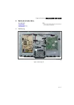
Page 9: ...ex of this chapter 4 1 Cable Dressing 4 2 Service Positions 4 3 Assembly Panel Removal 4 4 Set Re assembly Notes Figures below can deviate slightly from the actual situation due to the different set executions 4 1 Cable Dressing Figure 4 1 Cable dressing 32 19170_100_110705 eps 110705 ...

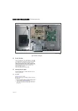
Page 10: ... display Caution Failure to follow these guidelines can seriously damage the display Ensure that ESD safe measures are taken 4 3 Assembly Panel Removal Instructions below apply to the 42PFL5606S 98 but will be similar for other models 4 3 1 Rear Cover Refer to Figure 4 3 for details Warning Disconnect the mains power cord before removing the rear cover 1 Remove the fixation screws 1 2 and 3 that s...

Page 11: ...2 Release the clamps and unplug all other connectors 2 3 Remove all fixation screws 3 from the SSB 4 Take out of the SSB Refer to Figure 4 4 for details Figure 4 4 SSB removal 4 3 3 Power Supply Unit PSU Caution it is mandatory to remount all different screws at their original position during re assembly Failure to do so may result in damaging the PSU 1 Unplug power connector from the SSB 2 Unplug...

Page 12: ...Take out the speakers as described earlier 3 Remove the MEMC board as described earlier 4 Remove the IR LED board as described earlier 5 Release all tapes that fit cables to the back side of the LCD panel 6 Remove all fixation screws of the sub frames on the sides of the LCD panel 7 Lift the sub frames together with the mounted panels from the LCD panel and put it aside 8 Lift the LCD panel from t...

Page 13: ...he rear cover Note For the new model range a new remote control RC is used with some renamed buttons This has an impact on the activation of the Service modes For instance the old MENU button is now called HOME or is indicated by a house icon 5 2 1 General Next items are applicable to all Service Modes or are general Life Timer During the life time cycle of the TV set a timer is kept called Op Hou...

Page 14: ...following methods Command MENU from the user remote will enter the normal user menu brightness contrast colour etc with SDM OSD remaining and pressing MENU key again will return to the last status of SDM again To prevent the OSD from interfering with measurements in SDM command OSD or i STATUS or INFO for NAFTA and LATAM from the user remote will toggle the OSD on off with SDM OSD remaining always...

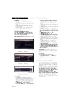
Page 15: ...s the call centre to diagnose problems and failures in the TV set before making a service call The CSM is a read only mode therefore modifications are not possible in this mode Main Menu Sub menu 1 Sub menu 2 Description System Information Op Hour This represents the life timer The timer counts normal operation hours but does not count Stand by hours Main SW ID e g TPM82A 1 02 See paragraph Softwa...

Page 16: ... Current Main SW Displays the built in main software version In case of field problems related to software software can be upgraded As this software is consumer upgradeable it will also be published on the Internet 2 2 Standby SW Displays the built in stand by processor software version Upgrading this software will be possible via USB 2 3 Panel Code Displays the Display Code number 2 4 NVM version...

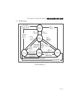
Page 17: ...ground tasks completed Swith On previously in Standby Semi Standby Mains Power Plug Standby Soft Mode Command Received Power tact switch Switch Off Mains Power Plug Switch Off Mains Power Plug Swith On previously in Standby Soft Mode Mains Power Plug Standby commands Received RC Standby key Standby Soft Mode Command Received previously in Standby Soft Mode Power tact switch TV Wakeup commands Rece...

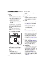
Page 18: ...rove its products and it s recommend that the TV software is updated when updates are available Software update files can be obtained from the dealer or can be downloaded from the following websites http www philips com support Preparing a portable memory for software upgrade The following requirements have to be met 1 A personal computer connected to the Internet 2 An archive utility that support...

Page 19: ... VAG_EDID_TPM83A_LA_CK BIN NVM NVM_TPM83A_LA_CK BIN For copying EDID data to the TV all 3 EDID files need to be available in repair directory 5 6 Error Codes 5 6 1 Introduction Error codes are required to indicate failures in the TV set In principle a unique error code is available for every Activated SW protection Failing I2C device General I2C error The last five errors stored in the NVM are sho...

Page 20: ...e entire error buffer is displayed when Service Mode SDM is entered 5 8 Fault Finding and Repair Tips Note It is assumed that the components are mounted correctly with correct values and no bad solder joints Before any fault finding actions check if the correct options are set 5 8 1 NVM Editor In some cases it can be convenient if one directly can change the NVM contents This can be done with the ...

Page 21: ...oup setting of colour temperature will be applied automatically to the TV VGA HDMI AV sources Table 6 1 White tone default settings 6 4 Option Settings 6 4 1 Introduction The microprocessor communicates with a large number of I2 C ICs in the set To ensure good communication and to make digital diagnosis possible the microprocessor has to know which ICs to address The presence absence of these MT53...

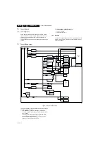
Page 22: ...n video decoder an audio decoder a dual link LVDS mini LVDS transmitter and an NTST PAL SECAM TV decoder with a 3D comb filter NTSC PAL 7 1 1 Implementation Key components of this chassis are MT5301B System On Chip SOC TV Processor F86WT 17 E Tuner analogue STA515W13TR Head Phone amplifier STA339BWTR audio amplifier TMDS361BPAGR HDMI switch 7 1 2 TPM8 3A Architecture Overview Figure 7 1 Architectu...

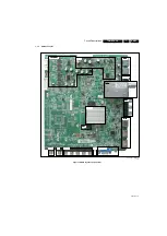
Page 23: ... EN 23 TPM8 3A LA 7 2011 Nov 11 7 1 3 SSB Cell Layout Figure 7 2 SSB layout cells top view 19170_206_110705 eps 111111 AUDIO CLASS SPDIF Video IN SPDIF MT5301B DDR2 HDMI AV IN USB AV OUT Component Analog Input TUNER DC DC ...

Page 24: ...ply for audio in active mode connector CN701 pins 8 and 9 19170_207_110704 eps 111107 MAX9728AETC U606 HP AMP STA339BWTR U602 AUDIO AMP STA515W U603 WOOFER AMP 5VSB VCCK 1 2V BUCK 3A G5657F12U U704 OPWRSB AO4449 Q707 5V_SW BUCK 3A TPS54319RTE U701 DVDD3V3 BUCK 1 5A SC189ASK U702 DDRV 1 5V LDO G903T63UF U705 B S 3 V 3 B S V 5 AO4449 Q709 12V LVDS_PWR_EN LDO G9084TU3U U7007 12V B_5V VCCK 1 2V NVRAM ...

Page 25: ...9 RLZ5 6B 1 2 FB701 120R 6000mA FB701 120R 6000mA R769 1K2 1 10W 5 R769 1K2 1 10W 5 R750 0R05 1 10W R750 0R05 1 10W C701 100UF 25V C701 100UF 25V R764 NC 1K 1 16W 5 R764 NC 1K 1 16W 5 R701 1 2K 1 16W R701 1 2K 1 16W C702 100N 50V C702 100N 50V C703 100UF 35V C703 100UF 35V 1 2 FB703 120R 6000mA FB703 120R 6000mA C704 100N 50V C704 100N 50V R712 0R05 1 10W R712 0R05 1 10W 19170_211_110705 eps 11072...

Page 26: ...22 0 1uF 50V C630 100UF 35V GND_SUB 1 SA 2 TEST_MODE 3 VSS 4 VCC_REG 5 OUT2B 6 GND2 7 VCC2 8 OUT2A 9 OUT1B 10 VCC1 11 GND1 12 OUT1A 13 GND_REG 14 VDD 15 CONFIG 16 OUT3B 17 OUT3A 18 EAPD OUT4B 19 TWARN OUT4A 20 VDD_DIG 21 GND_DIG 22 PWRDN 23 VDD_PLL 24 FILTER_PLL 25 GND_PLL 26 XTI 27 BICKI 28 LRCKI 29 SDI 30 RESET 31 INT_LINE 32 SDA 33 SCL 34 GND_DIG 35 VDD_DIG 36 Thermal Pad 37 U602 STA339BWTR C64...

Page 27: ...718 5V_SW 1 2 FB601 120R 6000mA 1 3 2 Q603 NC PDTC114ET R610 4K7 1 16W 5 R609 10K 1 16W 5 R602 NC 10K 1 16W 5 POP_MUTE D601 LL4148 D602 LL4148 5V_ON MUTE_CTL R608 1 8KOHM 1 10W R607 100R 1 16W 5 1 3 ZD601 BZX84C3V6 R603 1 8KOHM 1 10W C684 10uF 10V Q602 BC847C R601 100K 1 10W 5 R611 470KOHM 5 1 10W Q601 BC847C 19170_209_110705 eps 110705 3V3 Main Power 1 2 FB717 120R 3000mA C723 1UF 10V C722 1UF 10...

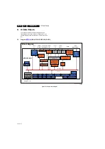
Page 28: ...eps 110623 Block diagram MT5301BCMU JPEG MP2 MP 4 DivX H 264 V C 1 RM AVS Component Analog Input 16 bit DDR2 DDR3 DRAM Bus JTAG IO Bus USB2 0 UART I 2 C PWM IrDA PCR SDIO Audio DSP NTSC PAL SECAM ATD Watchdog CVBS YC Input Audio I F SPDIF Out I2S RTC 2 D Graphic OSD scaler VADCx4 TV Decoder HDMI In I F LVDS OD mini LVDS TCON Audio Input Mix and Post Processing DDR2 DDR3 Controller BIM ARM11 HDMI R...

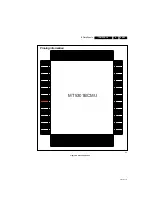
Page 29: ... Y0P AO1P 31 162 SOY0 AO1N 32 161 PR1P AO0P 33 160 PB1P AO0N 34 159 COM1 VCCK 35 158 Y1P VCCK 36 157 SOY1 VCCK 37 156 RP AVDD12_MEMPLL 38 155 COM AVSS12_MEMPLL 39 154 GP RODT RCKE 40 153 SOG RA8 RA10 41 152 BP RA13 RBA1 42 151 HSYNC RA11 RA4 43 150 VSYNC RA4 RA1 44 149 AVDD33_VGA_STB RA6 RA6 45 148 AVDD10_LDO RA0 RA8 46 147 ADIN4_SRV RA2 RA11 47 146 ADIN3_SRV RCAS_ RA12 48 145 ADIN2_SRV RCS_ RRAS_...

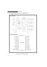
Page 30: ...4 33 32 31 30 29 28 27 26 25 24 23 22 21 20 19 VDD_DIG GND_DIG SCL SDA INT_LINE RESET SDI LRCKI BICKI XTI GND_PLL FILTER_PLL VDD_PLL PWRDN GND_DIG VDD_DIG TWARN OUT4A EAPD OUT4B GND_SUB SA TEST_MODE VSS VCC_REG OUT2B GND2 VCC2 OUT2A OUT1B VCC1 GND1 OUT1A GND_REG VDD CONFIG OUT3B FFX3B OUT3A FFX3A STA339BW Protection current thermal Logic Regulators Bias Power control FFX PLL Volume control Channel...

Page 31: ...UT1A OUT1A GND Reg VDD VDD CONFIG VL VSS VSS VCCSign VCCSign 18 16 17 15 6 5 4 3 2 21 22 31 32 33 35 34 36 20 1 19 N C GND Clean OUT1B VCC1B OUT1B PWRDN FAULT TRI STATE 9 8 7 28 29 30 OUT2A TH_WAR STA515W13TR 7 2 0 1 GND2B OUT2A VCC2A IN1A IN2B IN1B 14 12 11 23 25 26 GND2A IN2A 4 2 3 1 Logic I F and Decode LeftA Bridge Protection Circuitry INL 1 2 INR 1 2 PWRDN OUTPL FAULT VL TRI STATE OUTNL OUTPR...

Page 32: ...D S K N S _ D P H K N I 1 S L C S 48 47 46 45 44 43 42 41 40 39 38 37 36 35 34 33 D2 _1 D2 _1 VCC D1 _1 D1 _1 GND D0 _1 D0 _1 VCC CLK _1 CLK _1 SCL1 SDA1 HPD1 I2C_SEL S2 SDA 4 6 3 6 2 6 1 6 0 6 9 5 8 5 7 5 6 5 5 5 4 5 5 3 2 5 1 5 0 5 9 4 D P H 3 2 D 2 _ 2 _ 2 D V C C 1 D 2 _ 2 _ 1 D D N G 0 D 2 _ 2 _ 0 D V C C K L C 2 _ K L C 2 _ 2 L C S S 2 A D D P H 2 P L TMDS361B 64 pin TQFP HPD_SINK Vcc RINT C...

Page 33: ... LCD DISPLAY 1050 LCD DISPLAY 1050 CN414 40 LVDSVDD 39 LVDSVDD 38 LVDSVDD 37 LVDSVDD 36 SELLVDS 35 ODSEL 4 TX_AO0P 3 TX_AO1N 2 GND 1 TX_AO0N CN7003 5P CN7001 5P IR LED BOARD 1056 EMC CN401 1 LED_RED 2 LED_WGB 3 OIRI 4 GND 5 3V3SB 6 3V3SB 7 GND 8 KEY2 9 KEY 10 KEY 11 5VSB 12 LIT_SENSOR 13 GND CN602 1 ROUT 2 ROUT 3 LOUT 4 LOUT CN701 13 GND 12 5VSB 11 5VSB 10 STANDBY 9 24V 8 24V 7 GND 6 GND 5 GND 4 1...

Page 34: ...1 13 ON OFF 12 DIM 11 12V 10 12V 9 GND 8 GND 7 GND 6 24V 5 24V 4 PS_ON 3 5 2V 2 5 2V 1 CN9901 1 N 2 L AC Input MAIN POWER SUPPLY 1054 A J CN201 8P LEFT SPEAKER TO BACKLIGHT LCD DISPLAY 1050 RIGHT SPEAKER IR LED BOARD 1056 CN8104 12 VLED 11 VLED 10 LED3 9 LED4 8 LED6 7 LED8 6 LED7 5 LED5 4 LED2 3 LED1 2 VLED 1 VLED CN401 1 LED_RED 2 LED_WGB 3 OIRI 4 GND 5 3V3SB 6 3V3SB 7 GND 8 KEY2 9 KEY 10 KEY 11 ...

Page 35: ...Output COIXIAL PC IN DDC CVI VIDEO By CVI Y connector CVBS YPbPr RGB HDMI1 AUDIO IN PC AUDIO R L CVI CVBS 24C02 24C02 HDMI2 HDMI3 DDC DDC TMDS361 BPAGR SPDIF I2 S RX0 RX3 NAND FLASH 256 Mb CVBS AV Out WOOFER AMP STA515W SPK USB1 2 0 USB1 2 0 ATV DEMOD Analog IF TS SERIAL HDMI 1 3 ATV DTV RF TUNER TDTK T052D RESERVE Analog IF ATBM8848 RESERVE Demodulator Analog IF Side AV IN H Phone Out LVDS 50 60 ...

Page 36: ...F 160V 1 2 4 3 L9901 12MH L9901 12MH C9911 220pF 250V C9911 220pF 250V C9813 100N 50V C9813 100N 50V 1 2 t TH9902 SCK101R55LSY t TH9902 SCK101R55LSY C9815 330N 25V C9815 330N 25V C9816 2U2 16V C9816 2U2 16V L 1 N 2 CN9901 CONN CN9901 CONN 1 2 3 4 5 6 7 8 9 10 11 12 13 CN9002 CONN CN9002 CONN D9810 1N5408 11 D9810 1N5408 11 C9902 330NF 305V C9902 330NF 305V C9801 680NF C9801 680NF 1 2 3 4 5 6 7 8 9...

Page 37: ...2FD5T116 NC 1 2 4 5 6 7 8 9 10 T9301 POWER X FMR T9301 POWER X FMR R9335 100KOHM 5 1 8W R9335 100KOHM 5 1 8W C9318 2N2 50V C9318 2N2 50V R9306 330K 1 4W NC R9306 330K 1 4W NC R9328 1K5 1 8W 5 R9328 1K5 1 8W 5 1 2 3 4 IC9311 EL817M X IC9311 EL817M X R9324 47 OHM 1 4W R9324 47 OHM 1 4W R9302 330K 1 4W NC R9302 330K 1 4W NC D9310 UF4007 D9310 UF4007 R9331 1K OHM 5 1 8W R9331 1K OHM 5 1 8W C9311 10N 5...

Page 38: ...R9165 0 OHM 5 1 8W C9138 100PF C9138 100PF R9144 100K R9144 100K C9130 100N 50V C9130 100N 50V 1 2 D9131 SS0520 D9131 SS0520 1 2 D9132 SS0520 D9132 SS0520 C9131 100N 50V C9131 100N 50V C9147 1500PF NC C9147 1500PF NC L9122 Coil L9122 Coil R9158 100K R9158 100K R9142 0 1 ohm R9142 0 1 ohm C9133 4 7UF 50V C9133 4 7UF 50V C9141 1U 25V C9141 1U 25V R9188 18K 1 8W 1 R9188 18K 1 8W 1 C9140 1U 25V C9140 ...

Page 39: ...24 ZD8104 J9015 J9022 FB9811 J9036 L9901 L9902 HQ9801 CN8001 D9112 D9114 C9133 C9320 C9316 C9112 C9118 C9119 C9145 C9121 C9122 Q9801 BD9910 HQ8100 IC9301 J9046 J9039 J9018 HQ9121 J9025 R9143 R9142 D8100 R8110 R8111 J9014 J9017 J9009 J9001 J9043 J9027 J9023 R8137 ZD9300 C9142 D9113 D9111 J9007 J9021 J9019 J9003 C9147 J9012 J9011 T9301 L8100 C9920 C9925 C9146 HD9301 J9026 J9029 C9138 D9310 J9038 D93...

Page 40: ...3 R9165 R9166 R9167 R9169 R9188 R9319 R9321 R9322 R9328 R9333 R9334 R9329 R9144 R9145 R9148 R9149 R9157 R9158 R9323 R9324 IC8100 IC9801 R8100 JR9001 R9816 FD5 FD6 FD7 R8101 R8102 R8107 R8108 R8109 R8106 R8139 R8140 R8112 R8130 R8114 R8131 R8132 R8138 R8115 R8134 R8135 R8133 R8117 R8113 R9331 R9332 R8118 R8121 R8124 R8127 R9335 R8116 R8119 R8122 R8125 R8128 R9305 C8109 C8108 C8101 C8102 C8103 C8100...

Page 41: ... TVR14561KFC4FY RV9901 TVR14561KFC4FY 1 2 t NR9902 NTCR t NR9902 NTCR R9902 430K 1 4W R9902 430K 1 4W 1 2 HS9801 HEAT SINK Q9801 D9802 HS9801 HEAT SINK Q9801 D9802 1 2 3 4 HS9901 HEAT SINK BD9901 HS9901 HEAT SINK BD9901 C9911 220PF C9911 220PF 1 2 4 3 L9901 10MH L9901 10MH F9901 FUSE F9901 FUSE 1 2 FB9903 BEAD FB9903 BEAD R9903 430K 1 4W R9903 430K 1 4W C9902 470NF 305V C9902 470NF 305V 1 2 3 4 HS...

Page 42: ...48W D9306 1N4148W C9305 470uF 16V C9305 470uF 16V R9311 2 4 OHM 1 4W R9311 2 4 OHM 1 4W C9302 2N2 500V NC C9302 2N2 500V NC S OCP 1 BR 2 GND 3 FB OLP 4 VCC 5 D ST 7 D ST 8 IC9301 A6069H IC9301 A6069H R9309 1 5M 1 4W R9309 1 5M 1 4W C9306 100N 50V C9306 100N 50V C9307 100UF 35V C9307 100UF 35V C9313 10NF C9313 10NF 1 2 4 3 IC9302 PC123X8YFZOF IC9302 PC123X8YFZOF R9310 220 OHM 1 4W R9310 220 OHM 1 4...

Page 43: ...ZOF IC9802 PC123X8YFZOF C9801 680NF C9801 680NF R9804 680K OHM 1 1 4W R9804 680K OHM 1 1 4W C9805 47P 50V C9805 47P 50V 1 2 ZD9801 MTZJ T 72 16B ZD9801 MTZJ T 72 16B R9811 13K 1 8W 1 R9811 13K 1 8W 1 R9809 680K OHM 1 1 4W R9809 680K OHM 1 1 4W Q9807 NC Q9807 NC 1 2 t NR9801 NTCR t NR9801 NTCR C9811 470N 25V C9811 470N 25V INV 1 COMP 2 RAMP 3 CS 4 ZCD 5 GND 6 OUT 7 VCC 8 IC9801 LD7591GS IC9801 LD75...

Page 44: ...1 Coil R9222 47OHM 5 1 8W R9222 47OHM 5 1 8W C9220 220pF 50V C9220 220pF 50V C9215 1U 25V C9215 1U 25V C9216 1U 50V C9216 1U 50V R9216 2M 1 1 4W R9216 2M 1 1 4W 1 2 D9207 RB160M 60TE25 D9207 RB160M 60TE25 R9211 5 1KOHM 1 1 8W R9211 5 1KOHM 1 1 8W C9217 10pF3KV C9217 10pF3KV 1 2 3 D9205 FMW 2156 D9205 FMW 2156 1 2 ZD9202 MTZJ T 72 24B ZD9202 MTZJ T 72 24B R9205 7 5 OHM 1 4W R9205 7 5 OHM 1 4W R9220...

Page 45: ... OC 6 RC 7 Reg 8 RV 9 COM 10 VGL 11 NC 12 NC 13 VB 14 VS 15 VGH 16 NC 17 NC 18 IC9101 SSC9512S TL IC9101 SSC9512S TL C9103 1N 50V C9103 1N 50V R9115 16K9 1 8W 1 R9115 16K9 1 8W 1 1 2 ZD9104 MTZJ T 72 15B ZD9104 MTZJ T 72 15B C9120 100NF 50V C9120 100NF 50V 1 2 D9103 RB160M 60TE25 D9103 RB160M 60TE25 R9127 34K R9127 34K R9122 47OHM 5 1 8W R9122 47OHM 5 1 8W 1 2 3 D9102 FMX 23S D9102 FMX 23S R9106 3...

Page 46: ... BAV70 D8103 BAV70 1 2 ZD8114 MTZJ T 72 NC ZD8114 MTZJ T 72 NC R8134 10K 1 8W R8134 10K 1 8W 1 2 ZD8112 MTZJ T 72 NC ZD8112 MTZJ T 72 NC R8156 12R 1 R8156 12R 1 R8159 0R05OHM1 8W R8159 0R05OHM1 8W R8108 5 1R 1 R8108 5 1R 1 3 2 1 D8107 BAW56 D8107 BAW56 C8106 1UF NC C8106 1UF NC R8110 51K 1 4W NC R8110 51K 1 4W NC S2 1 G2 2 S1 3 G1 4 D1 5 D1 6 D2 7 D2 8 Q8104 AO4828L Q8104 AO4828L 1 2 ZD8110 MTZJ T...

Page 47: ...D8114 ZD8115 ZD8108 ZD8113 J918 J969 J933 C9901 C9902 RV9901 NR9801 NR9902 NR9901 L9801 T9201 T9101 J970 T9301 R8127 C9314 GND4 GND6 GND9 J948 J914 HS9801 HS9201 HS9202 HS9901 R1 R2 BD9901 C9101 C9106 C9111 C9113 C9116 C9117 C9202 C9203 C9205 C9206 C9207 C9208 C9217 C9219 C9222 C9304 C9307 C9310 C9313 C9801 C9802 C9803 C9804 C9911 C9912 C9913 C9914 D9301 D9303 D9304 D9801 F9901 FB9101 FB9102 FB980...

Page 48: ...R9224 R9225 R9226 R9302 R9303 R9304 R9305 R9306 R9307 R9308 R9309 R9310 R9311 R9312 R9313 R9314 R9315 R9316 R9317 R9318 R9319 R9320 R9802 R9803 R9804 R9805 R9806 R9807 R9809 R9810 R9811 R9812 R9813 R9814 R9815 R9816 R9817 R9818 R9901 R9902 R9903 Q8101 Q8102 Q8103 Q8104 Q8105 Q8106 Q8107 Q8108 IC9101 IC8101 IC8102 R8121 R8122 R9123 R9124 R9125 JR901 JR902 JR903 JR904 JR907 JR908 JR910 JR911 JR912 J...

Page 49: ... PWM Control L BL_ON H BL_OFF 0 Max Luma 99 Min Luma R746 4K7 1 16W 5 R744 10K 1 16W 5 R706 2 2K 1 16W R712 0R05 1 10W R751 0R05 1 10W 1 2 CN416 NC CONN R703 10K 1 16W 5 R750 0R05 1 10W Q703 PMBS3904 R765 NC 1K 1 16W 5 C705 100UF 25V R764 NC 1K 1 16W 5 C702 100N 50V C707 100N 16V C701 100UF 25V R709 1K 1 16W 5 C704 100N 50V 1 2 ZD139 RLZ5 6B R711 47K 1 16W 5 R702 NC 10K 1 16W 5 1 2 3 4 5 6 7 8 9 1...

Page 50: ...20R 6000mA C758 NC 10U 16V VI 3 VO 2 GND 1 4 4 U708 U708 R728 C745 2 2nF 50V R737 15K 1 R743 2 7K 1 16W 1 C7003 22UF 1 2 FB729 120R 3000mA S 1 S 2 S 3 G 4 D 8 D 7 D 6 D 5 Q707 AO4449 7A 30V C737 10U 16V C761 NC 10U 16V C763 NC 10U 16V L701 1 5UH R715 10K 1 16W 5 C715 NC 220NF 25V 1 2 FB717 120R 3000mA FB717 1 2 FB727 120R 3000mA R725 56KOHM 1 16W LX 1 BST 2 GND 3 FB 4 COMP 5 EN 6 VIN 7 VBIAS 8 U70...

Page 51: ... 1 6 2 7 3 8 4 9 5 11 12 13 14 15 10 17 16 C116 R159 75R 1 16W 1 U105 CAT24C02YI GT3 I A0 1 A1 2 A2 3 GND 4 SDA 5 SCL 6 WP 7 VCC 8 R166 0R05 1 16W C118 10N 50V 1 2 R167 NC 10K 1 16W 5 R158 68R 1 16W 5 R188 1K 1 16W 5 C117 ZD122 NC MLVG0402 1 2 ZD123 123 1 2 R176 5 1K 1 R182 NC 2K 1 16W 1 ZD129 1 2 ZD125 1 2 R157 75R 1 16W 1 Q105 PMBS3904 ZD117 1 2 D103 NC BAS316 A 1 K 2 1 2 ZD130 1 2 ZD118 NC MLVG...

Page 52: ... 4W C150 10uF 16V C150 10uF 16V 1 2 ZD132 NC MLVG0402 ZD132 NC MLVG0402 C157 10nF50V C157 10nF50V R227 470K 1 16W 5 R227 470K 1 16W 5 1 2 ZD133 NC MLVG0402 ZD133 NC MLVG0402 R225 18R 1 16W 5 R225 18R 1 16W 5 R222 10K 1 16W 5 R222 10K 1 16W 5 1 2 ZD103 NC MLVG0402 ZD103 NC MLVG0402 1 2 FB106 120R 3000mA FB106 120R 3000mA C107 47nF 16V C107 47nF 16V C110 10N 50V C110 10N 50V C101 10U 10V C101 10U 10...

Page 53: ... 16W 1 R559 NC 100R 1 16W 1 R551 1K 1 16W 5 R551 1K 1 16W 5 C501 10U 10V C501 10U 10V R554 4K7 1 10W 5 R554 4K7 1 10W 5 1 2 ZD502 NC MLVG0402 ZD502 NC MLVG0402 A 1 K 2 D512 NC BAS316 D512 NC BAS316 R522 NC 0R05 1 16W R522 NC 0R05 1 16W SDA3 1 SCL3 2 GND 3 CLK _3 4 CLK _3 5 VCC 6 D0 _3 7 D0 _3 8 GND 9 D1 _3 10 D1 _3 11 VCC 12 D2 _3 13 D2 _3 14 GND 15 VSadj 16 D2 _SINK 17 D2 _SINK 18 VCC 19 D1 _SINK...

Page 54: ...55 33R 1 16W 5 R1155 33R 1 16W 5 R1141 0R05 1 16W R1141 0R05 1 16W Q1101 NC PMBS3904 Q1101 NC PMBS3904 1 2 3 Q1108 PMBS3906 Q1108 PMBS3906 R1191 100K 1 16W 5 R1191 100K 1 16W 5 R1133 0R05 1 16W R1133 0R05 1 16W R1189 NC 0R05 1 16W R1189 NC 0R05 1 16W R1156 33R 1 16W 5 R1156 33R 1 16W 5 R1140 4K7 1 16W 5 R1140 4K7 1 16W 5 R1137 NC 4K7 1 16W 5 R1137 NC 4K7 1 16W 5 R1160 51R 1 16W 5 R1160 51R 1 16W 5...

Page 55: ...309 NC 15K 1 16W 5 R309 NC 15K 1 16W 5 3 1 2 D301 NC BAV99 D301 NC BAV99 R306 22K R306 22K 1 2 FB307 NC 120R 3000mA FB307 NC 120R 3000mA R305 47K R305 47K R304 22K R304 22K 1 2 t TH301 PTCR t TH301 PTCR 1 2 3 4 5 7 8 6 CN103 USB CONN CN103 USB CONN R307 0R05 1 16W R307 0R05 1 16W 3 1 2 D303 NC BAV99 D303 NC BAV99 1 2 3 4 5 6 7 8 1 2 3 4 CN104 USB CONN 1 2 3 4 CN104 USB CONN C311 10U 16V C311 10U 1...

Page 56: ... Standby Power System IO STBY GPIO AADC ADC in GPIO Normal GPIO HDMI_S2 H H H HDMI B L HDMI A HDMI C L L HDMI_S1 Strapping GPIO R436 0R05 1 16W R436 0R05 1 16W R413 0R05 1 16W R413 0R05 1 16W R423 100R 1 16W 5 R423 100R 1 16W 5 R420 0R05 1 16W R420 0R05 1 16W C434 100N16V C434 100N16V R412 1 3K 1 R412 1 3K 1 C409 100N16V C409 100N16V R402 NC 10K 1 16W 5 R402 NC 10K 1 16W 5 FSRC_WR 1 VCC3IO 3 GPIO1...

Page 57: ...K 1 16W 5 R474 NC 10K 1 16W 5 R458 NC 10K 1 16W R458 NC 10K 1 16W CS 1 SO SIO1 2 WP SIO2 3 GND 4 SI SIO0 5 SCLK 6 NC SIO3 7 VCC 8 U404 NC MX25L6445EM2I 10G U404 R480 NC 1M 1 16W R480 NC 1M 1 16W R467 NC 5K1 1 16W 5 R467 NC 5K1 1 16W 5 GND 1 RESET 2 VCC 3 U406 MAX809STRG U406 MAX809STRG R461 10K 1 16W 5 R461 10K 1 16W 5 R471 NC 6K8 1 10W 1 R471 NC 6K8 1 10W 1 C452 NC 10U 10V C452 NC 10U 10V R469 0R...

Page 58: ...M0 12 1_A6 12 RDQ1 12 Damping for DDR2 1 ADDR CMD Damping Termination for CLK CAPs Close to DDR2 1 DDR2 1 64Mx16 1066MHz J1 A1 E1 R1 E9 G7 G9 A9 C7 C9 G1 G3 C1 C3 J9 M9 C469 100N16V C469 100N16V C466 100N16V C466 100N16V R483 100R 1 16W 5 R483 100R 1 16W 5 C470 100N16V C470 100N16V 1 2 3 4 8 7 6 5 RP401 100 OHM 1 16W RP401 100 OHM 1 16W R481 0R05 1 16W R481 0R05 1 16W C467 100N16V C467 100N16V R48...

Page 59: ... 12 TX_AECKP 12 TX_AECKN 12 U0TX 6 12 U0RX 6 12 OSCL0 8 9 10 12 13 18 20 OSDA0 8 9 10 12 13 18 20 M_TX_AE4P 22 M_TX_AE4N 22 M_TX_AE3P 22 M_TX_AE3N 22 M_TX_AECKN 22 M_TX_AECKP 22 M_TX_AE2N 22 M_TX_AE2P 22 M_TX_AE1P 22 M_TX_AE0N 22 M_TX_AE0P 22 M_TX_AE1N 22 M_TX_AO3N 22 M_TX_AO3P 22 M_TX_AO4N 22 M_TX_AO4P 22 M_TX_AO2P 22 M_TX_AOCKN 22 M_TX_AOCKP 22 M_TX_AO2N 22 M_TX_AO0P 22 M_TX_AO1N 22 M_TX_AO1P 22...

Page 60: ...5 1 16W 1 2 FB202 120R 3000mA FB202 120R 3000mA 1 2 FB201 120R 3000mA FB201 120R 3000mA R201 1MOHM 1 16W 5 R201 1MOHM 1 16W 5 C205 100N 16V C205 100N 16V C207 33P 50V C207 33P 50V R206 NC 4K7 1 16W 5 R206 NC 4K7 1 16W 5 R202 100R 1 16W 5 R202 100R 1 16W 5 Q201 NC 2N7002 Q201 NC 2N7002 R203 100R 1 16W 5 R203 100R 1 16W 5 C204 100N 16V C204 100N 16V C206 100N 16V C206 100N 16V 1 2 3 4 5 6 7 8 9 10 1...

Page 61: ...5 1 2 CN122 RCA JACK CN122 RCA JACK INR 1 INR 2 OUTL 12 UVP 11 PVDD 9 PVSS 6 EN 5 SGND 4 OUTR 3 INL 14 CN 7 CP 8 PGND 10 INL 13 U413 NC DRV603PWR U413 NC DRV603PWR C141 47pF 50V C141 47pF 50V C1306 NC 1UF16V C1306 NC 1UF16V R1302 NC 100OHM1 16W R1302 NC 100OHM1 16W R1313 NC 47K1 16W R1313 NC 47K1 16W L101 1 8 uH L101 1 8 uH R1310 NC 47K1 16W R1310 NC 47K1 16W R1325 NC 10K1 16W R1325 NC 10K1 16W C1...

Page 62: ... 50V D605 LL4148 D605 LL4148 C620 0 1uF 50V C620 0 1uF 50V R630 2R2 1 16W 5 R630 2R2 1 16W 5 R617 10K 1 16W 5 R617 10K 1 16W 5 R633 2K2 1 1 16W R633 2K2 1 1 16W C683 10UF C683 10UF C614 47pF 50V C614 47pF 50V 1 2 FB617 120R 6000mA FB617 120R 6000mA C630 100UF 35V C630 100UF 35V R601 100K 1 10W 5 R601 100K 1 10W 5 D606 LL4148 D606 LL4148 C633 1N 50V C633 1N 50V C685 100UF 35V C685 100UF 35V C632 0 ...

Page 63: ...R1137 R114 R1140 R1141 R1142 R1143 R1144 R1145 R1146 R1147 R1148 R1149 R115 R1150 R1153 R1154 R1155 R1156 R1157 R1158 R1159 R199 R1160 R1166 R1183 R1185 R1188 R1191 R205 R226 R215 R225 R126 R212 R128 R222 R200 R183 R218 R223 R216 R224 R227 R214 R140 R141 R142 R143 R144 R145 R146 R147 R149 R150 R151 R152 R153 R154 R156 R157 R159 R163 R164 R165 R166 R167 R170 R210 R173 R174 R175 R176 R177 R178 R179 ...

Page 64: ...C1113 C1115 C1116 C1117 C1118 C1120 C1121 C1122 C1123 C1124 C1126 C1142 C1143 C1147 C155 C406 C407 C408 C410 C4104 C4105 C411 C4112 C4113 C4114 C4115 C4121 C4123 C4124 C4126 C4127 C4128 C4129 C4130 C4135 C4137 C416 C417 C418 C4191 C4199 C421 C422 C423 C424 C425 C453 C204 C463 C464 C465 C466 C467 C468 C469 C470 C471 C504 C505 C506 C507 C508 C509 C516 C780 C118 C119 C149 C151 C154 C157 C158 C132 C13...

Page 65: ...858 EMC Board 311GW250B05BBX RC_IR_OUT TXD1 ITV_VDD_C RXD1 ITV_VDD ITV_VDD ITV_VDD R4402 10K 1 16W 5 CN7001 CONN 1 2 3 4 5 R4401 100R 1 16W 5 ZD135 NC MLVG0402 1 2 t TH4401 8V 0R4 1 2 ZD137 NC MLVG0402 1 2 C4401 100N 16V R4414 0R05OHM1 16W NC ZD138 NC MLVG0402 1 2 ZD136 NC MLVG0402 1 2 Q4401 2N3906S RTK PS 1 2 3 CN7003 CONN 1 2 3 4 5 6 7 R4403 10K 1 16W 5 ...

Page 66: ...011 Nov 11 EMC board layout 19170_530_110629 eps 110722 2011 06 21 1 715G4858 EMC board layout top bottom CN1 C4401 CN7003 Q4401 R4401 R4402 R4403 R4414 ZD135 ZD136 ZD137 ZD138 R5 R6 R11 R12 CN7001 R13 Layout EMC Board Top Side Layout EMC Board Bottom Side ...

Page 67: ... 16W 5 R231 NC 15K 1 16W CB201 TOUCH PAD 9X15 1 R203 560R 1 16W 5 R212 10K 5 1 16W CN201 CONN 1 2 3 4 5 6 7 8 9 10 R238 NC 2M OHM 1 16W 5 R220 1K CB204 TOUCH PAD 9X15 1 C203 0 47UF 10V CB202 TOUCH PAD 9X15 1 R202 560R 1 16W 5 R226 39R 1 C208 1UF16V C214 NC 100P 50V ZD201 NC UDZSNP3 3B 1 2 R204 560R 1 16W 5 R227 NC 22K U201 CG7216AM 1 2 3 4 5 6 7 8 9 10 11 12 13 14 15 16 P2 5 P2 1 P1 7 P1 5 P1 3 P1...

Page 68: ... bottom CB205 CB201 CB202 CB203 CB204 CB206 U202 LED201 U203 C201 C202 C203 C204 C208 Q201 R201 R202 R203 R204 R208 R213 R205 R212 R220 R225 CN202 R210 CN201 C209 R226 ZD201 C211 C210 R228 C207 R222 R223 R224 C212 C213 C214 R227 R229 R230 R231 R232 R233 R234 R235 R236 R237 R238 R239 R240 U205 U201 Layout IR LED Board Top Side Layout IR LED Board Bottom Side ...

Page 69: ...1 2011 Nov 11 11 Styling Sheets 11 1 Ebony 32 19170_800_110702 eps 110702 Ebony 32 Pos No Description Remarks 30 BEZEL 40 REAR COVER 50 BASE ASSY 1176 REMOTE CONTROL FOR ELECTRICAL PARTS ASSEMBLIES SEE WIRING DIAGRAM CHAPTER 9 40 50 30 ...

Page 70: ...ing Sheets 2011 Nov 11 11 2 Ebony 42 19170_801_110702 eps 110702 Ebony 42 Pos No Description Remarks 30 BEZEL 40 REAR COVER 50 BASE ASSY 1176 REMOTE CONTROL FOR ELECTRICAL PARTS ASSEMBLIES SEE WIRING DIAGRAM CHAPTER 9 30 50 40 ...

Reviews: