162
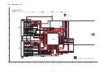
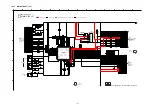
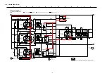
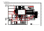
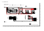
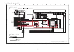
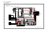
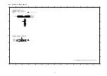
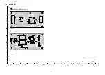
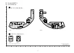
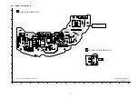
18.1.14. WIRELESS ADAPTER CIRCUIT
: +B SIGNAL LINE
: AUDIO OUTPUT SIGNAL LINE
TO DIGITAL TRANSMITTER
C
TO
MAIN CIRCUIT
(CN4701)
IN SCHEMATIC
DIAGRAM - 7
F
WIRELESS ADAPTER CIRCUIT
SCHEMATIC DIAGRAM - 14
SC-ZT2EE/GS(SU-ZT2EE/GS) WIRELESS ADAPTER
CIRCUIT
E
TO
POWER SW
CIRCUIT (TP4612*)
IN SCHEMATIC
DIAGRAM - 13
A
1
2
3
4
5
6
7
8
9
10
11
12
13
14
1
2
3
4
5
6
7
8
9
10
11
12
13
14
C
D
B
E
G
H
F
A
C
D
B
E
G
H
F
C4718
0
10
C4720
0.1
C4719
7
8
5
6
9
24
14
16
15
11
12
10
13
22
23
19
20
17
18
21
2
1
4
3
26
25
CN4703
TP4701*
100P
C4701
100
R4713
LB4721
J0JBC0000014
100
R4709
2.7K
R4705
1000P
C4709
100P
C4705
100P
C4713
R4701
4.7K
18
16
14
8
9
11
12
10
2
3
1
5
7
6
4
13
15
17
19
CN4702
R4703
4.7K
LB4723
J0JBC0000014
C4721
6.3V1200
100P
C4704
R4715
100
R4707
2.7K
R4711
100
R4712
100
R4716
100
100P
C4716
LB4724
J0JBC0000014
R4708
2.7K
100P
C4708
1000P
C4712
R4704
4.7K
R4702
4.7K
100
R4710
2.7K
R4706
100
R4714
1000P
C4710
100P
C4714
LB4722
J0JBC0000014
100P
C4702
100P
C4706
1000P
C4711
100P
C4715
100P
C4703
100P
C4707
SCL
SD0
SDI
SM0
SM1
AGND
SSB
INT
WM_DET
5V_GND
ADC_V
CH4_R_IN
CH4_L_IN
+5V
AGND
AGND
AGND
AGND
CH3_R_OUT
CH1_R_OUT
CH1_L_OUT
CH3_L_OUT
AGND
AGND
CH2_R_OUT
CH2_L_OUT
SSB
SCL
INT
+5V
SD0
PGND
AGND
+7VA
AGND
AGND
AGND
AGND
AGND
WM_DET
SDI
CH1_R_OUT
CH1_L_OUT
CH2_R_OUT
CH2_L_OUT
19
1
Summary of Contents for VIERA Link SB-ZT2EE
Page 10: ...10 5 Location of Controls and Components 5 1 Main Unit SU ZT2 ...
Page 11: ...11 5 2 Speaker Unit SB ZT2 5 3 Remote Control ...
Page 12: ...12 6 Installation ...
Page 13: ...13 6 1 Basic Connections 6 1 1 Connecting equipment with HDMI terminal TV DVD recorder etc ...
Page 14: ...14 6 1 2 Connecting equipment without HDMI terminal DVD player VCR etc ...
Page 15: ...15 6 1 3 Connecting STB etc and audio terminals DVD player etc ...
Page 16: ...16 6 1 4 Other connections ...
Page 17: ...17 6 2 AC power supply connection ...
Page 18: ...18 7 Speaker setting SB ZT2 7 1 Setting the speakers Front and Surround speakers ...
Page 19: ...19 ...
Page 20: ...20 7 2 Setting surround speakers ...
Page 28: ...28 9 2 2 Speaker Unit SB ZT2 ...
Page 29: ...29 9 2 3 Speaker Unit SB ZT2 Wireless Link ...
Page 30: ...30 ...
Page 32: ...32 ...
Page 33: ...33 10 1 Main Parts Location Diagram 10 1 1 Main Unit SU ZT2 ...
Page 34: ...34 10 1 2 Speaker Unit SB ZT2 ...
Page 36: ...36 10 2 2 Speaker Unit SB ZT2 ...
Page 49: ...49 Step 4 Remove the Weight ...
Page 50: ...50 Step 5 Remove 10 screws ...
Page 54: ...54 Step 11 Remove 2 screws Step 12 Lift up to remove Arm Cover A ...
Page 56: ...56 Step 14 Tilt the Woofer Block in order as arrows shown to detach it from the Tweeter Block ...
Page 67: ...67 Step 3 Remove the heatsink with the IC5701 ...
Page 68: ...68 Step 4 Remove 1 screw Step 5 Remove IC5701 from the heatsink ...
Page 70: ...70 Step 4 Place the heatsink with the IC5701 onto the SMPS P C B ...
Page 82: ...82 Step 4 Remove 3 screws Step 5 Remove the Power Button ...
Page 87: ...87 Step 3 Remove 4 screws Step 4 Lift up to remove Woofer Speaker SP1 ...
Page 111: ...111 Step 11 Remove 3 screws ...
Page 112: ...112 Step 12 Remove the Light Panel Step 13 Remove the Power Button ...
Page 113: ...113 Step 14 Hold on to the P C B Holder and lift up the Input P C B as arrow shown ...
Page 114: ...114 Step 15 Place the D Amp P C B and Input P C B on an insulation sheet ...
Page 132: ...132 ...
Page 133: ...133 14 Overall Simplified Block 14 1 Signal Flow SU ZT2 ...
Page 144: ...144 ...
Page 148: ...148 ...
Page 168: ...168 ...
Page 176: ...176 ...
Page 178: ...178 ...
Page 182: ...182 ...


