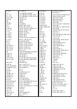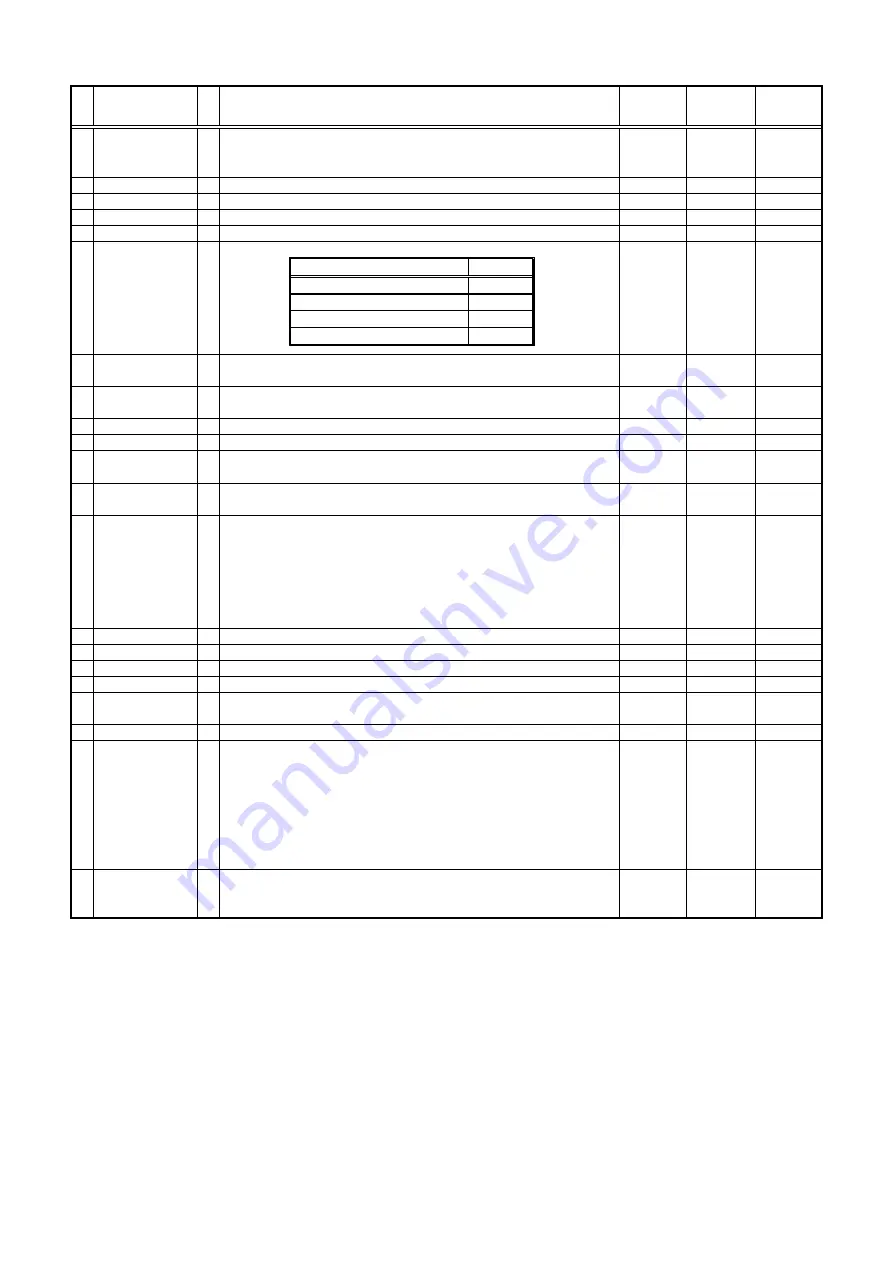
No Terminal Name I/O
Description
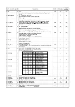
P.OFF
P.Failure
Reset/
Release
1
PROGRESSIVE TV
(L)
I
Port for scanning line control:
scanning line 628: H
scanning line 624: L
Low
Low
Low
2 CODE1
I
AD input terminal for model setting.
In
In
In
3 CODE2
I
AD input terminal for model setting.
In
In
In
4 T.S.CUREVE
I
Input terminal for "S-Curve" of Tuner AFC at channel selecting.
In
In
In
5 NC
O Low fix.
Low
Low
Low
6 NORM/SERV/T2/TEST I
Factory mode/ Service mode setting terminal.
In
In
In
7 S-PHOTO
I
Input terminal of the Tape End sensor detection.
*More than 2.6V : Black tape part. *Less than 2.4V :Trans. Tape part.
In
In
In
8 T-PHOTO
I
Input terminal of the Tape Beginning sensor detection.
*More than 2.6V : Black tape part. *Less than 2.4V :Trans. Tape part.
In
In
In
9 TRACKING_ENVE
I
Input terminal of the Video envelope signal.
In
In
In
10 NC
O Low fix.
Low
Low
Low
11 CURRENT.LIMIT
O
Control terminal for the Capstan current limit.
(Output impedance: MIN:1K, TYP:2.5K, MAX:4.0K)
In
DA=0V
Low
In
DA=0V
12 EEPROM_CS
O
Chip Select terminal for NAVI Data backup EEPROM.
*Active Low output.
High
Low
Low
13 ART.V/H/N
O
Output terminal for the Artificial V-sync.
1. In trick playback.
Artificial V sync inserting timing : High
Artificial H sync inserting timing : Hi-Z (M output)
Except above conditions : Low
2. NAVI REC : Hi-Z
3. OSD REC : Hi-Z
4. Other than above conditions : Low
Low
Low
Low
14 REMOCON
I
Input terminal for the Remote Controller.
In
In
In
15 PICT1
O Control terminal for the Picture mode.
Low
Low
Low
16 NC
O Low fix.
Low
Low
Low
17 PICT2
O Control terminal for the Picture mode.
Low
Low
Low
18 VIDEO.H.SW
O
Video head switching signal
*L'/R="High" *R'/L="Low"
Low
Low
Low
19 AUDIO.H.SW
O Head switching signal for Audio circuit.
Low
Low
Low
20 D.FM.REC
O
Recording control signal for Hi-Fi Audio signal.
*REC, INSERT, AV INSERT:"High" is output. (Rec on)
*Other than above condition: "Low" is output. (Rec off)
*From L to H: Switching timing of this signal is synchronized with the HSW edge just
after switching timing of "D33 of IC3001 = 0 to 1". (The delay is within 1 edge)
*From H to L: When Editing, this switching timing is before the switching timing of
"D33 of IC3001 = from 1 to 0" by 60 +- 10msec in SP mode, by 100 +- 10msec in
LP/EP mode. When normal rec mode, this switching timing is before the switching
timing of "D33 of IC3001 = from 1 to 0" by 0 ~ 150msec.
Low
Low
Low
21 R_COLE_W (L)
O
Write protection releasing terminal for RAM correction EEPROM.
*During ROM correction data being Written: "Low" is output.
*Other than above condition: Hi-Z.
Hi-Z
Hi-Z
Hi-Z
Input Voltage
Mode
Over 4.0V
Normal
Over 2.0V and less than 4.0V Service
Over 1.0V and less than 2.5V Test 2
Less than 1.0V
Test 1
Summary of Contents for NV-HV61GN
Page 21: ...2 REMOVAL OF THE BACK PANEL Remove 2 Screws C Remove Screw D Unlock 4 Tabs E Fig D3 21 ...
Page 29: ...10 2 CASING PARTS SECTION 29 ...
Page 30: ...10 3 PACKING PARTS SECTION 30 ...
Page 31: ...11 REPLACEMENT PARTS LIST 31 ...
Page 41: ...C4537 ECJ2VC1H560G CHIP CAPACITOR 41 ...
Page 44: ...D2002 B0AAED000003 DIODE 44 ...
Page 47: ...Q1152 2SC3311ASA TRANSISTOR 47 ...
Page 49: ...R1502 ERJ3GEYJ273V CHIP RESISTOR 49 ...
Page 54: ...W519 ERJ3GEY0R00V CHIP JUMPER 54 ...
Page 109: ...4 1 3 PARTS NAME OF R4 MECHANISM Fig M2 ...
Page 139: ...34 ...


