Confidential
Until : Indefinite
Specifications
MN34120PAJ
Total Page
Page
96
86
2015/10/01
Generalplus Technology Inc.
Enactment Revision
Panasonic Semiconductor Solutions Co., Ltd.
■
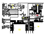
Notes of terminal processing
Layout about the power supply wiring and the peripheral parts.
-The separation of the power supply and GND is different according to the board of Set. Above figure is one
example for reference.
-The grounded capacitance values for “CAPD1,VCHP1,VCHP2,VCHP3” are the recommended values when
designing. There is a possibility of changing the value in the future.
-The test land (TL) at BIASO is a test terminal for the management analysis. Please install the TL-pin when
there is allowable space.
-The grounded capacitor for “CAPD1” must be used temperature property B rank (±10%) more over.
-The grounded capacitor for “VCHP1,CHP2,VCHP3” must be used temperature property B rank (±10%)
more over.
-Please use temperature property B rank (±10%) more over for the decoupling capacitor of the power supply.
-Between the power supply and GND becoming a pair, please arrange the decoupling capacitor (0.01
μ
F) in
the terminal neighborhood as much as possible.
-Since the decoupling capacitor inserted in the power supply is a reference value and different according to
the board of Set, It should be optimize.
-All terminals of power supply and GND in sensor should be processed.


