33
KX-TG6700BXB/KX-TGA670BXB
4.9.4.
5.8 GHz PA (Power Amplifier), 5.8 GHz LNA (Low Noise Amplifier) and Antenna
Switch Circuit
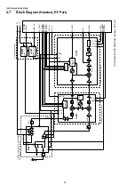
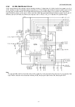
PA block amplifies power of 5.8 GHz TX signal.
5.8 GHz TX signal from 5.8 GHz Converter circuit is filtered by 5.8 GHz-BPF FL811, and amplified by Power amplifier (PA) block of
IC851. After that, it is supplied to Antenna Switch block of IC851. V_PA is approximately 4.0 V at Base Unit, and 3.1 V at Handset.
LNA block amplifies receiving 5.8 GHz signal.
5.8 GHz RX signal from Antenna Switch block of IC851 amplified by LNA (Low Noise Amplifier) block of IC851 and filtered by HPF
(FL821), and then supplied to 5.8 GHz Converter circuit.
Antenna Switch block selects the TX 5.8 GHz signal or RX 5.8 G signal, and connect to Antenna terminal.
Note:
The exposed GND_PLATE on the bottom of the IC851 supplies the circuit ground(s) for the entire chip. It is very important that
a good solder connection is made between this GND_PLATE and the ground plane of the PCB underlying the IC851.
<Base Unit>
IC851 includes Switches for High frequency signals, and controlled by ANT0 signal and ANT1 signal from DSP.
DSP is checking RSSI (Received Signal Strength Indicator) signal, and selects better condition Antenna from two antennas.
At the TX mode 5.8 GHz TX signal from 5.8 GHz PA block leads to selected Antenna terminal, at the RX mode 5.8 GHz RX signal
from selected Antenna terminal leads to 5.8 GHz LNA block.
<Handset>
IC851 includes Switch for High frequency signals, and controlled by PA_CONT signal and RX_EN signal from DSP. At the TX mode
5.8 GHz TX signal from 5.8 GHz PA block leads to Antenna terminal, at the RX mode 5.8 GHz RX signal from Antenna terminal
leads to 5.8 GHz LNA block.
Summary of Contents for KX-TG6700BXB
Page 2: ...2 KX TG6700BXB KX TGA670BXB ...
Page 6: ...6 KX TG6700BXB KX TGA670BXB 3 Specifications ...
Page 35: ...35 KX TG6700BXB KX TGA670BXB 4 11 Signal Route Each signal route is as follows ...
Page 36: ...36 KX TG6700BXB KX TGA670BXB RF part signal route ...
Page 40: ...40 KX TG6700BXB KX TGA670BXB 6 1 2 Connecting the Telephone Line Cord ...
Page 41: ...41 KX TG6700BXB KX TGA670BXB 6 1 2 1 If you subscribe to a DSL service ...
Page 43: ...43 KX TG6700BXB KX TGA670BXB 6 4 1 Battery Level 6 4 2 Panasonic Battery Performance ...
Page 46: ...46 KX TG6700BXB KX TGA670BXB ...
Page 47: ...47 KX TG6700BXB KX TGA670BXB 7 2 2 Programming Using the Direct Commands ...
Page 48: ...48 KX TG6700BXB KX TGA670BXB ...
Page 49: ...49 KX TG6700BXB KX TGA670BXB 7 3 Error Messages ...
Page 50: ...50 KX TG6700BXB KX TGA670BXB 7 4 Troubleshooting ...
Page 51: ...51 KX TG6700BXB KX TGA670BXB ...
Page 52: ...52 KX TG6700BXB KX TGA670BXB ...
Page 72: ...72 KX TG6700BXB KX TGA670BXB 10 1 9 5 RF DSP Interface Signal Wave Form Test Burst Mode ...
Page 73: ...73 KX TG6700BXB KX TGA670BXB Test Burst Mode ...
Page 80: ...80 KX TG6700BXB KX TGA670BXB 11 1 2 Handset ...
Page 81: ...81 KX TG6700BXB KX TGA670BXB 11 1 3 Charger Unit ...
Page 93: ...93 KX TG6700BXB KX TGA670BXB Memo ...
Page 97: ...97 KX TG6700BXB KX TGA670BXB Memo ...
Page 106: ...106 KX TG6700BXB KX TGA670BXB Memo ...
Page 116: ...116 KX TG6700BXB KX TGA670BXB 15 3 Explanation of IC Terminals RF Part 15 3 1 IC701 ...
Page 117: ...117 KX TG6700BXB KX TGA670BXB 15 3 2 IC801 Backside Terminal GND ...
Page 118: ...118 KX TG6700BXB KX TGA670BXB 15 3 3 IC851 Backside Terminal GND ...
Page 122: ...122 KX TG6700BXB KX TGA670BXB 16 3 Cabinet and Electrical Parts Charger Unit ...
Page 123: ...123 KX TG6700BXB KX TGA670BXB 16 4 Accessories and Packing Materials 16 4 1 KX TG6700BXB ...
Page 124: ...124 KX TG6700BXB KX TGA670BXB 16 4 2 KX TGA670BXB ...

