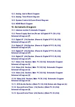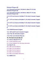
Schematic Diagram (S)
13.14. Syscon/Servo/Timer (3/4) Section (Main P.C.B.(3/4))
Schematic Diagram (S)
13.15. Syscon/Servo/Timer (4/4) Section (Main P.C.B.(3/4))
Schematic Diagram (S)
13.16. I/O Tuner Section (1/4) (Main P.C.B.(4/4)) Schematic Diagram
(I)
13.17. I/O Tuner Section (2/4) (Main P.C.B.(4/4)) Schematic Diagram
(I)
13.18. I/O Tuner Section (3/4) (Main P.C.B.(4/4)) Schematic Diagram
(I)
13.19. I/O Tuner Section (4/4) (Main P.C.B.(4/4)) Schematic Diagram
(I)
13.20. HDMI Schematic Diagram
13.21. SD Card/DV Jack Schematic Diagram
13.22. Front (R) Schematic Diagram
13.23. Front (L) Schematic Diagram
14. Printed Circuit Board
14.1. Power & Digital I/F P.C.B.
14.1.1. Power & Digital I/F P.C.B.
14.1.2. Power & Digital I/F P.C.B. Address Information
14.2. Main P.C.B.
14.2.1. Main P.C.B. (1/4 Section)
14.2.2. Main P.C.B. (2/4 Section)
14.2.3. Main P.C.B. (3/4 Section)
14.2.4. Main P.C.B. (4/4 Section)
14.2.5. Main P.C.B. Address Information
14.3. HDMI P.C.B.
62
Summary of Contents for DMR-ES45VP
Page 7: ...3 Service Navigation 3 1 Service Information 4 Specifications 7 ...
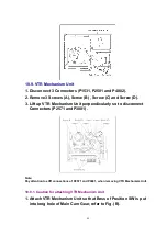
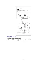
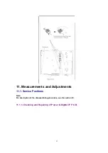
Page 68: ...10 13 Main P C B 1 Disconnect 5 Connectors 2 Remove 2 Screws A and remove Main P C B 52 ...
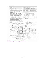
Page 70: ...11 1 2 Checking and Repairing of Main P C B 54 ...
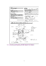
Page 71: ...11 1 3 Checking and Repairing of RAM Digital P C B Module 55 ...
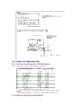
Page 73: ...11 2 3 Items that should be done after replacing parts 57 ...
Page 74: ...58 ...
Page 75: ......
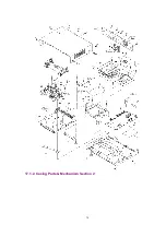
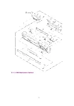
Page 87: ...17 1 2 Casing Parts Mechanism Section 2 70 ...
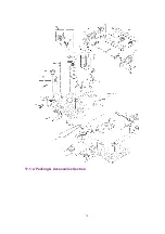
Page 88: ...17 1 3 VHS Mechanism Section 71 ...
Page 89: ...17 1 4 Packing Accessories Section 72 ...
Page 111: ...C11701 F2A1A2220055 10V 2200U 1 94 ...
Page 123: ......
Page 124: ......
Page 132: ...1 4 2 4 3 4 4 4 DMR ES45VP ES46VP Main P C B VEPV0054BT 4 4 Section Location Map REAR FRONT ...

