CDV Construction Manual – Issue 3
Page 13
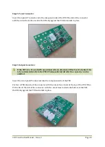
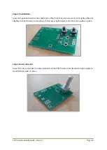
Step 2: Power Connector
Insert the 4 pin JST connector into the component side of the PCB. The side of the connector
with the cutout faces the encoder. Hold firmly against the PCB and solder in place.
Step 3: Output Connectors
If the CDV is to be used with an optional add-on attenuator filter board, decide if it is
to be soldered directly to the PCB. If being soldered directly the connector can be
omitted.
Insert the two 2 pin JST connectors into the component side of the PCB.
For Rev. A PCB the side of the connector with the cutout faces towards the top of the PCB. If the
PCB is Rev. B the side of the connector with the cutout faces towards the bottom of the PCB.
Hold firmly against the PCB and solder in place.
Summary of Contents for CDV
Page 1: ...CDV Construction Manual Issue 3 Page 1 CDV COMPACT DIGITAL VFO CONSTRUCTION MANUAL ...
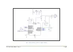
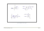
Page 8: ...CDV Construction Manual Issue 3 Page 8 Figure 1 Microcontroller and power supply schematic ...
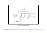
Page 9: ...CDV Construction Manual Issue 3 Page 9 Figure 2 Si5351A Clock generator schematic ...
Page 10: ...CDV Construction Manual Issue 3 Page 10 Figure 3 Display and controls schematic ...
Page 30: ...CDV Construction Manual Issue 3 Page 30 Figure 11 Attenuator filter board fitted to the CDV ...


