CDV Construction Manual – Issue 3
Page 12
6
C
ONSTRUCTION
6.1
G
ENERAL
The CDV is built on a high quality fibreglass PCB. The PCB is doubled sided with tracks on both
sides but with the top side mainly forming a ground plane.
Components are loaded into the PCB from both sides. When the component side is mentioned in
the following instructions it refers to the side of the PCB where the SMD parts are installed. The
reverse side is referred to as the solder side.
To assist construction the PCB has a screen printed component overlay and a solder mask to
help guard against solder bridges.
The components are static sensitive. Use anti-static measures when handling the
PCB out of its protective bag.
6.2
S
TEPS
Step 1: PCB
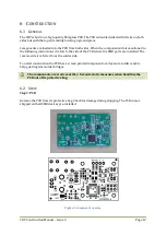
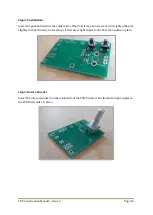
Remove the PCB from its protective bag. Check for damage during shipping. The PCB comes
shipped with all SMD devices pre-installed.
Figure 4 Component overlay
Summary of Contents for CDV
Page 1: ...CDV Construction Manual Issue 3 Page 1 CDV COMPACT DIGITAL VFO CONSTRUCTION MANUAL ...
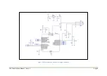
Page 8: ...CDV Construction Manual Issue 3 Page 8 Figure 1 Microcontroller and power supply schematic ...
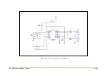
Page 9: ...CDV Construction Manual Issue 3 Page 9 Figure 2 Si5351A Clock generator schematic ...
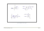
Page 10: ...CDV Construction Manual Issue 3 Page 10 Figure 3 Display and controls schematic ...
Page 30: ...CDV Construction Manual Issue 3 Page 30 Figure 11 Attenuator filter board fitted to the CDV ...


