


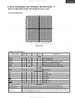

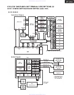
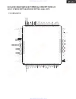
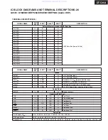


Q3701,Q3721,Q3741,Q3761,Q3781: PCM1796DBR (24 bit, 192 kHz, 2ch DAC)
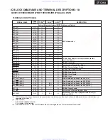
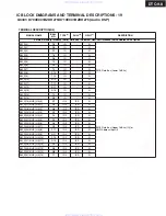
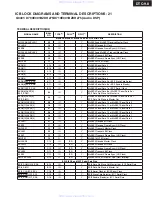
TERMINAL DESCRIPTION
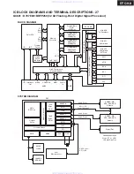
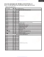
IC BLOCK DIAGRAMS AND TERMINAL DESCRIPTIONS -14
DTC-9.8
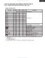
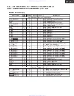
TERMINAL
I/O
DESCRIPTIONS
NAME
PIN
I/O
DESCRIPTIONS
AGND1
19
–
Analog ground (internal bias)
AGND2
24
–
Analog ground (internal bias)
AGND3L
27
–
Analog ground (L-channel DACFF)
AGND3R
16
–
Analog ground (R-channel DACFF)
BCK
6
I
Bit clock input(1)
DATA
5
I
Serial audio data input(1)
DGND
8
–
Digital ground
IOUTL+
25
O
L-channel analog current
IOUTL–
26
O
L-channel analog current output–
IOUTR+
17
O
R-channel analog current
IOUTR–
18
O
R-channel analog current output–
IREF
20
–
Output current reference bias pin
LRCK
4
I
Left and right clock (fS) input(1)
MC
12
I
Mode control clock input(1)
MDI
11
I
Mode control data input(1)
MDO
13
I/O
Mode control readback data output(3)
MS
10
I/O
Mode control chip-select input(2)
MSEL
3
I
I2C/SPI select(1)
RST
14
I
Reset(1)
SCK
7
I
System clock input(1)
VCC1
23
–
Analog power supply, 5 V
VCC2L
28
–
Analog power supply (L-channel DACFF), 5 V
VCC2R
15
–
Analog power supply (R-channel DACFF), 5 V
VCOML
22
–
L-channel internal bias decoupling pin
VCOMR
21
–
R-channel internal bias decoupling pin
–
Digital power supply, 3.3 V
I/O
Zero flag for L-channel(2)
I/O
Zero flag for R-channel(2)
(1) Schmitt-trigger input, 5-V tolerant
(2) Schmitt-trigger input and output. 5-V tolerant input and CMOS output
(3) Schmitt-trigger input and output. 5-V tolerant input. In I2C mode, this pin becomes an open-drain 3-state output; otherwise, this pin is a CMOS
www. xiaoyu163. com
QQ 376315150
9
9
2
8
9
4
2
9
8
TEL 13942296513
9
9
2
8
9
4
2
9
8
0
5
1
5
1
3
6
7
3
Q
Q
TEL 13942296513 QQ 376315150 892498299
TEL 13942296513 QQ 376315150 892498299


