


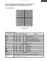

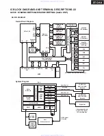
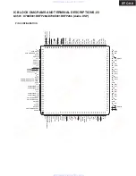
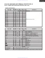
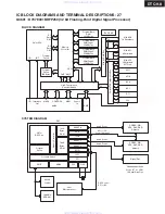

IC BLOCK DIAGRAMS AND TERMINAL DESCRIPTIONS -12
Q4305: NJU7313AM (Analog Function Switch)
BLOCK DI AGRAM
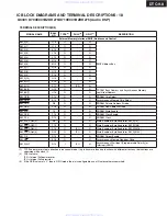
TERMINAL DESCRIPTION
DTC-9.8
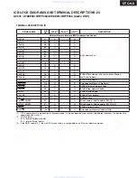
L1
L2
L3
L4
L-COM1
L5
L6
L-COM2
L7
L8
L-COM3
ST
R1
R3
R2
R4
R-COM1
R5
R6
R-COM2
R7
R8
R-COM3
CK
DATA
VSS
VDD
VEE
Pin No.
Pin Name
Description
10
11
12
14
15
16
17
19
20
21
22
23
24
25
26
27
28
29
30
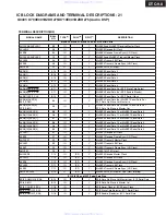
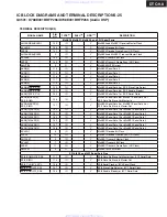
Pin No.
Pin Name
Description
L7
L8
L-COM3
ST
VSS
CK
DATA
R-COM3
R8
R7
R-COM2
R6
R5
R-COM1
R4
R3
R2
R1
VDD
Negative Voltage Supply
Analog switch input/output
Analog switch input/output
L7, L8 Common
Chip enable
GND
Clock input
Data input
R7, R8 Common
Analog switch input/output
Analog switch input/output
R5, R6 Common
Analog switch input/output
Analog switch input/output
R1, R2, R3, R4 Common
Analog switch input/output
Analog switch input/output
Analog switch input/output
Analog switch input/output
Positive voltage supply
Control Circuit
Latch Circuit
Le
v
el Shifter
Latch Circuit
Le
v
el Shifter
www. xiaoyu163. com
QQ 376315150
9
9
2
8
9
4
2
9
8
TEL 13942296513
9
9
2
8
9
4
2
9
8
0
5
1
5
1
3
6
7
3
Q
Q
TEL 13942296513 QQ 376315150 892498299
TEL 13942296513 QQ 376315150 892498299


