


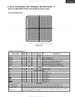

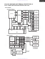

BLOCK DIAGRAM
TERMINAL DESCRIPTION
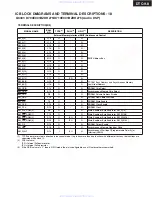
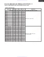
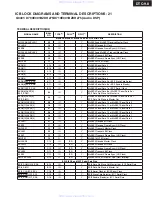
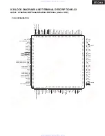
IC BLOCK DIAGRAMS AND TERMINAL DESCRIPTIONS -10
Q4306: NJU7311AM(Analog Function Switch)
DTC-9.8
L1
L2
L-COM1
L3
L4
L-COM2
L5
L6
L-COM3
L7
L-COM4
ST
R1
R-COM1
R2
R3
R4
R-COM2
R5
R6
R-COM3
R7
R-COM4
CK
DATA
VSS
VDD
VEE
Latch Circuit
Le
v
el Shifter
Control Circuit
Latch Circuit
Le
v
el Shifter
10
11
12
14
15
16
17
19
20
21
22
23
24
25
26
27
28
29
30
L-COM3
L7
L-COM4
ST
VSS
CK
DATA
R-COM4
R7
R-COM3
R6
R5
R-COM2
R4
R3
R-COM1
R2
R1
VDD
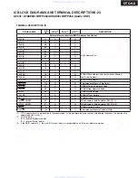
Pin No.
Pin Name
Description
Pin No. Pin Name
Description
Negative Voltage Supply
L5, L6 Common
Analog switch input/output
L7 Common
Chip enable
GND
Clock input
Data input
R7 Common
Analog switch input/output
R5, R6 Common
Analog switch input/output
Analog switch input/output
R3, R4 Common
Analog switch input/output
Analog switch input/output
R1, R2, Common
Analog switch input/output
Analog switch input/output
Positive voltage supply
www. xiaoyu163. com
QQ 376315150
9
9
2
8
9
4
2
9
8
TEL 13942296513
9
9
2
8
9
4
2
9
8
0
5
1
5
1
3
6
7
3
Q
Q
TEL 13942296513 QQ 376315150 892498299
TEL 13942296513 QQ 376315150 892498299


