


MCU_CAN_TXD
MCU_CAN_RXD
MCU_GPIO
INH
CANH
CANL
Vbatt
+5V
+5V
10K Ω
10K Ω
TJA1054
INH
1
WAKE
7
STB
5
EN
6
TXD
2
ERR
4
RXD
3
G
N
D
1
3
RTL
9
CANH
11
CANL
12
RTH
8
B
A
T
1
4
V
C
C
1
0
4700 pF
++
10 uF
4700 pF
++
10 uF
511 Ω
120 Ω
511 Ω
MCU_GPIO
MCU_GPIO
Isolation and protection circuitry is not shown
in this drawing,only a termination resistor is shown.
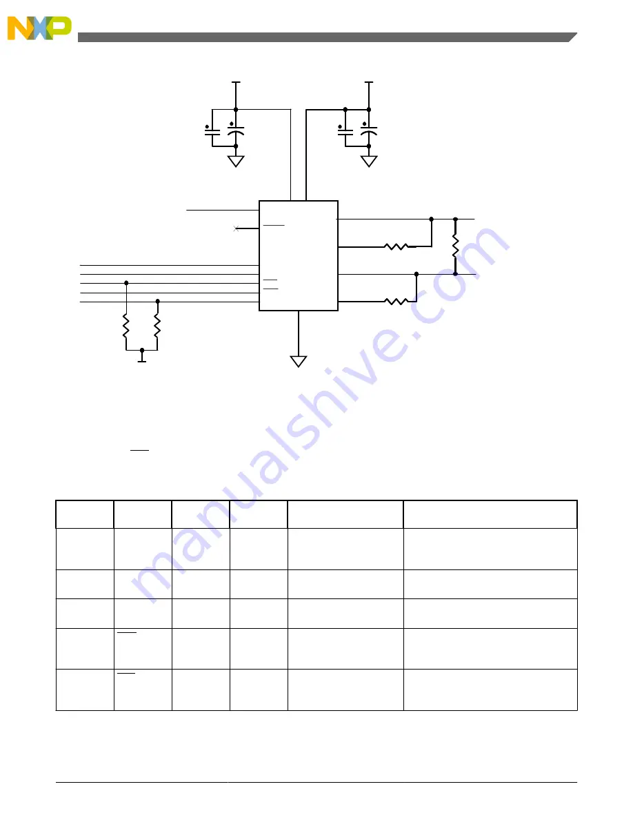
Figure 10. Typical low-speed CAN circuit using TJA1054
NOTE
Decoupling shown as an example only.
STB and EN should be pulled high for Normal mode. These signals can optionally be
connected to MCU GPIO pins to allow MCU control of the the physical interface.
Table 17. TJA1054 pin definitions and example system connections
Pin
number
Pin name
Pin
direction
Full pin
name
MCU or system
connection
Description
1
INH
Input
Inhibit
Typically not connected
Inhibit output for control of an external
power supply regulator if a wake up
occurs.
2
TXD
Input
Transmit
Data
MCU CAN TXD
CAN transmit data input from the MCU.
3
RXD
Output
Receive
Data
MCU CAN RXD
CAN receive data output to the MCU.
4
ERR
Output
Error
MCU GPIO
The error signal indicates a bus failure
in normal operating mode or a wake up
is detected in standby or sleep modes.
5
STB
Input
Voltage
Supply for
IO
MCU GPIO
Standby input for device. It is also used
in conjunction with the EN pin to
determine the mode of the transceiver.
Table continues on the next page...
Example communication peripheral connections
Hardware Design Guide, Rev. 0, 2012
Freescale Semiconductor, Inc.
19


