


NOTE
Decoupling shown as an example only.
TXD/RXD pullup/pulldown may be required, depending on device implementation.
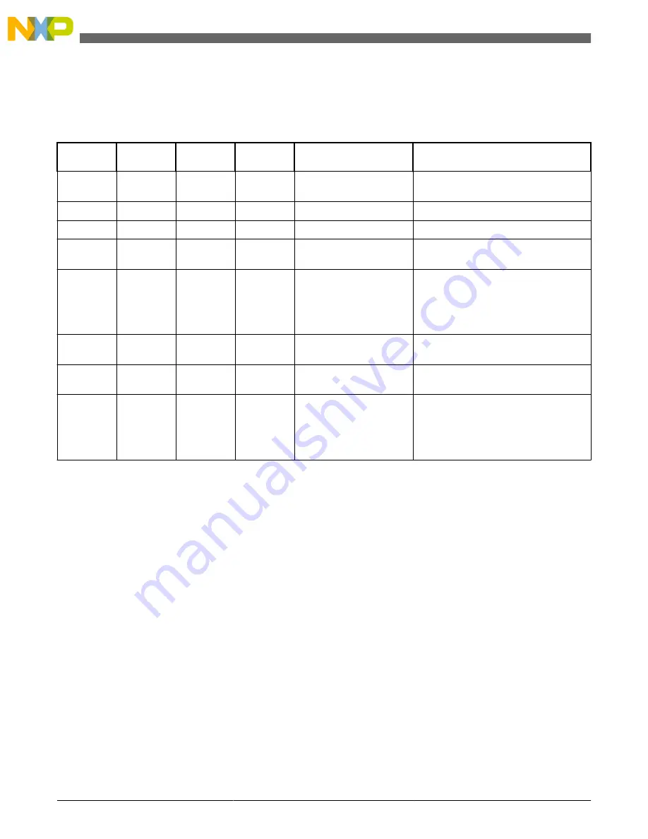
Table 16. TJA1050 pin definitions and example system connections
Pin
number
Pin name
Pin
direction
Full pin
name
MCU or system
connection
Description
1
TXD
Input
Transmit
Data
MCU CAN TXD
CAN transmit data input from the MCU.
2
GND
Output
Ground
Ground
Ground return termination.
3
VCC
Input
5 V
Voltage supply input (5 V).
4
RXD
Output
Receive
Data
MCU CAN RXD
CAN receive data output to the MCU.
5
VREF
Output
Reference
voltage
Output
Not used
Mid-supply output voltage. This is
typically not used in many systems, but
can be used if voltage translation needs
to be done between the CAN
transceiver and the MCU.
6
CANL
Input/
Output
CAN Bus
Low
CAN Bus Connector
CAN bus low pin.
7
CANH
Input/
Output
CAN Bus
High
CAN Bus Connector
CAN bus high pin.
8
S
Input
Select
Grounded or MCU GPIO
Select for high-speed mode or silent
mode. Silent mode disables the
transmitter, but keeps the rest of the
device active. This may be used in the
case of an error condition.
8.2.2 Low-speed CAN TJA1054 interface
Figure 10
shows the typical connections for the physical interface between the MCU and the CAN bus for LS applications
using the NXP TJA1054 LS CAN transceiver. Optionally, the standby and enable pins can be connected to MCU GPIO pins
for additional control of the physical interface.
Example communication peripheral connections
Hardware Design Guide, Rev. 0, 2012
18
Freescale Semiconductor, Inc.


