background image

Nvis 5586A 


Nvis Technologies Pvt. Ltd. 

28 


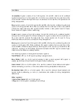
• 

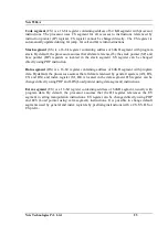
Overflow Flag 

(OF):


 set if the result is too large positive number, or is too small negative 

number to fit into destination operand. 
 
• 

Direction Flag 

(DF)

If set then string manipulation instructions will auto-decrement index 

register. If cleared then the index registers will be auto-incremented. 
 
• 

Interrupt-enable Flag 

(IF)

Setting this bit enables maskable interrupts. 

 
• 

Single-step  Trap  Flag 

(TF)

  If  set  then  single-step  interrupt  will  occur  after  the  next 

instruction. 
 
• 

Sign Flag 

(SF)

Set if the most significant bit of the result is set. 

 
• 

Zero Flag 

(ZF)

Set if the result is zero. 

Auxiliary carry Flag 

(AF)

Set if there was a carry  from or borrow to bits 0-3  in the  AL 

register. 
 
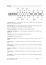
• 

Parity Flag 

(PF) - set if parity (the number of "1" bits) in the low-order byte of the result is 

even. 
 
• 

Carry Flag 

(CF) - set if there was a carry from or borrows to the most significant bit during 

last result calculation. 
 
• 

Auxiliary carry Flag 

(AF) - set if there was a carry from or borrows to bits 0-3 in the AL 

register. 
 
• 

Parity Flag 

(PF) - set if parity (the number of "1" bits) in the low-order byte of the result is 

even. 
 
• 

Carry Flag 

(CF) - set if there was a carry from or borrows to the most significant bit during 

last result calculation. 


Summary of Contents for 5586A

Page 1: ...Nvis 5586A Learning Material Ver 1 0 Designed Manufactured by 141 B Electronic Complex Pardesipura Indore 452 010 India Tel 91 731 4211500 Telefax 91 731 4202959 Toll free 1800 103 5050 E mail info n...

Page 2: ...Nvis 5586A Nvis Technologies Pvt Ltd 2...

Page 3: ...8 Memory Address Port Address 65 9 Subroutines 68 10 Serial Communication 95 11 MASM Macro Assembler 100 12 Sample Programs 104 13 On Board Interface 163 14 Parallel Communication between two Nvis 558...

Page 4: ...packed up with powerful monitor in 128K Bytes of factory programmed EPROMS and 32K Bytes of Read Write Memory The total memory on the board is 144K Bytes The system has 72 programmable I O lines The...

Page 5: ...ing three nos of 8255 Serial RS 232 C Interface using 8251 Interrupt 8 different level interrupt using 8259 Timer Counter Three 16 bit Timer Counter using 8253 Keyboard Display 105 IBM PC Keyboard 20x...

Page 6: ...nly the mains cord designed for this instrument Ensure that the mains cord is suitable for your country Ground the Instrument This instrument is grounded through the protective earth conductor of the...

Page 7: ...o provide internal timing 8086 is designed to operate in two modes Minimum and Maximum It can prefetches upto 6 instruction bytes from memory and queues them in order to speed up instruction execution...

Page 8: ...ture of 8086 8086 has two blocks BIU and EU The BIU performs all bus operations such as instruction fetching reading and writing operands for memory and calculating the addresses of the memory operand...

Page 9: ...BIU is free to look ahead in the program by prefetching the next sequential instruction These prefetching instructions are held in its FIFO queue With its 16 bit data bus the BIU fetches two instruct...

Page 10: ...cycles to memory or I O and perform the operation specified by the instruction on the operands During the execution of the instruction the EU tests the status and control flags and updates them based...

Page 11: ...and I O interface The minimum mode signal can be divided into the following basic groups address data bus status control interrupt and DMA Address Data Bus These lines serve two functions As an addres...

Page 12: ...ata for I O devices and interrupt type codes from an interrupt controller Status signal The four most significant address lines A19 through A16 are also multiplexed but in this case with status signal...

Page 13: ...M IO tells external circuitry whether a memory or I O transfer is taking place over the bus Logic 1 at this output signals a memory operation and logic 0 an I O operation The direction of data transfe...

Page 14: ...RESET to logic 0 initializes the internal register of the 8086 and initiates a reset service routine DMA Interface signals The direct memory access DMA interface of the 8086 minimum mode consist of th...

Page 15: ...bus cycle is to follow S2 S1 S0 are input to the external bus controller device the bus controller generates the appropriately timed command and control signals The 8288 chip receive the status signal...

Page 16: ...f the 1 st three signals are the same as those in the minimum mode The signal MCE PDEN has 2 functions depending on the mode in which 8288 is operating The 8288 can either operate in I O bus mode or s...

Page 17: ...he code 111 is output by the 8086 it is signaling that no bus activity is to take place The control outputs produced by the 8288 are DEN DT R and ALE These 3 signals provide the same functions as thos...

Page 18: ...is used for monitor storage while RAM for user s program storage A system may contain I O devices The clock generator generates the clock from the crystal oscillator and then shapes it and divides to...

Page 19: ...ding the address in T1 the processor sends the data to be written to the addressed location The data remains on the bus until middle of T4 state The WR becomes active at the beginning of T2 unlike RD...

Page 20: ...previous cycle or during T1 state of the current cycle the CPU activates HLDA in the next clock cycle and for succeeding bus cycles the bus will be given to another requesting master The control of th...

Page 21: ...ut depends upon the status of the IOB pin If IOB is grounded it acts as master cascade enable to control cascade 8259A else it acts as peripheral data enable used in the multiple bus configurations IN...

Page 22: ...AMWC or AIOWC is activated from T2 to T4 and MWTC or IOWC is activated from T3 to T4 The status bit S0 to S2 remains active until T3 and become passive during T3 and T4 If reader input is not activat...

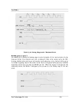
Page 23: ...Nvis 5586A Nvis Technologies Pvt Ltd 23 Memory Read Timing in Maximum Mode...

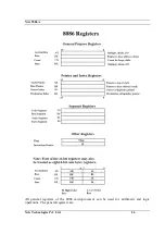
Page 24: ...ent registers The 8086 has a total of fourteen 16 bit registers including a 16 bit register called the status register with 9 of bits implemented for status and control flags Most of the registers con...

Page 25: ...an be changed directly using POP instruction Data segment DS is a 16 bit register containing address of 64KB segment with program data By default the processor assumes that all data referenced by gene...

Page 26: ...Nvis 5586A Nvis Technologies Pvt Ltd 26 All general registers of the 8086 microprocessor can be used for arithmetic and logic operations The general registers are...

Page 27: ...Data register consists of two 8 bit registers DL and DH which can be combined together and used as a 16 bitregister DX When combined DL register contains the low order byte of the word and DH contain...

Page 28: ...SF Set if the most significant bit of the result is set Zero Flag ZF Set if the result is zero Auxiliary carry Flag AF Set if there was a carry from or borrow to bits 0 3 in the AL register Parity Fl...

Page 29: ...ddress formed by adding an 8 bit or 16 bit displacement with the content of any one of the registers BX BP SI and DI in the default either DS or ES segment Example MOV AX 50H BX 6 Indexed Addressing M...

Page 30: ...Nvis 5586A Nvis Technologies Pvt Ltd 30...

Page 31: ...Machine Control Instructions These instructions control the machine status NOP HLT WAIT and LOCK instructions belong to this class 6 Flag Manipulation Instructions All the instructions which directly...

Page 32: ...ne by prefixing instructions with the DS CS SS or ES some registers and instructions by default may use the ES or SS segments instead of DS segment Word data can be located at odd or even byte boundar...

Page 33: ...flow interrupt interrupts due to INT instructions etc Non Maskable Interrupt The processor 8086 has a non maskable interrupt input pin NMI that has the highest priority among the external interrupts T...

Page 34: ...Nvis 5586A Nvis Technologies Pvt Ltd 34 the next instruction The status of the pending interrupts is checked at the end of each instruction cycle...

Page 35: ...byte locations 2 Examine Modify the contents of any of internal register of 8086 3 Move a block of Data Program from one location to another location 4 Fill a particular memory area with a constant 5...

Page 36: ...ernal SMPS Power Supply to AC Power and 5 pin connector to the left side on Nvis 5586A Kit 2 Switch on the Power Supply at the rear end of SMPS supply 3 A message NV5586A 8086 Mic Tr will come on disp...

Page 37: ...terrupt an interrupt vector pointer must be provided on the data bus when INTA is active An interrupt Controller Circuit is provided to take care of more than one source of interrupt Co Processor 8087...

Page 38: ...his is selected by a set of jumpers JP3 on the right hand side of the 8284 clock generator as shown below 1 2 MHz UPPER 2 CLK 3 1 MHz LOWER The Nvis 5586A is supplied in 2 MHz configuration Bus Contro...

Page 39: ...and then converts them into a continuous serial data stream for transmission Simultaneously it can receive serial data stream and converts them into parallel data characters for the CPU This chip wil...

Page 40: ...ular will automatically increase or decrease the words in order to move to different addresses The user can therefore continue sending in word code The cursor as to moved around or moved in the right...

Page 41: ...n register stores the instruction code and address information which contains display data RAM and address of character generator RAM However the content of IR is only for read in but not read out The...

Page 42: ...hat the LCD Modular is executing the inner instruction and no other instruction can be accepted The LCD Modular can only accept information when BF is lower to 0 Address Counter A C The address counte...

Page 43: ...t character code The shape and code are shown in Table 2 and 3 Character Generator RAM C G RAM This RAM stores 8 different 5x7 dot of array character which allows the user to design the program When t...

Page 44: ...Nvis 5586A Nvis Technologies Pvt Ltd 44 Character Codes Note 1 The CG RAM generates character patterns in accordance with the user s program 2 Shaded areas indicate 5x10 dot character patterns...

Page 45: ...Nvis 5586A Nvis Technologies Pvt Ltd 45 Character code Note 1 The CG RAM generates character patterns in accordance with the user s program 2 Shaded areas indicate 5x10 dot character patterns...

Page 46: ...or 5x7 Signifies a don t care bit Note 1 Character code bits 0 2 correspond to CG RAM address bits 3 5 Each of the 8 unique bit strings designated one of the 8 character patterns 2 A CG RAM address bi...

Page 47: ...a light dot in the corresponding position on the display panel Functions of Reset Using the Internal Reset Circuit to Start LCD Modular internal has an automatic power supply to be used to RESET when...

Page 48: ...Nvis 5586A Nvis Technologies Pvt Ltd 48 Diagram of module RESET power Instruction Set Note...

Page 49: ...edetermined for each model Initialization by Instructions If the power conditions for the normal operation of the internal reset circuit are not satisfied LCD unit must be initialized by executing a s...

Page 50: ...command will put the display data into a empty space code 20H address counter will be cleared to 0 When executing this command display OFF the cursor or the character blinking function will be moved...

Page 51: ...be sent into the CPU and character generator RAM D D RAM Address Set Address counter and display data RAM have addresses which are driven by the binary 7 bit When this instruction is driven in data ca...

Page 52: ...to be used again in order to read the D D RAM data The data can be read from the C G RAM D D RAM after the cursor shift After the execution of data address counter add 1 or minus 1 will be set in the...

Page 53: ...ys used to move the cursor around Move one space to the left Delete the character at the cursor Simply Press the key A After the command an A will appear on the screen Assembly language can be input a...

Page 54: ...screen if not switch off the power supply and re check The following steps are to be taken 1 Press the key A and the LCD display is as shown here 2 Now the user enter the segment address and effectiv...

Page 55: ...ory location 2 Or user has entered the wrong instruction as follows As user press the Enter key then above instruction will not be converted into machine language And the cursor will point left side o...

Page 56: ...hen this input assemble language will be converted into machine language in the memory and jump to the next memory location Now write the next instruction as follows In this way user can enter the who...

Page 57: ...address If press the Enter or the ARROW UP key after specifying the address the memory will display the data Press ARROW UP key will allowed the address to ADD 8 and store in the memory as a whole nu...

Page 58: ...is the starting position G Proceed to the address for execution The GO command which causes the machine language statements to be executed This command executes the loaded program and allows the user...

Page 59: ...y allows interruption to be shown on the screen Note 1 During interrupt setting the address alternation register has commands like POP ES MOV DS AS etc to execute with the next command 2 The program w...

Page 60: ...ther press G Enter and then F7 This indicates the third break point is at 0411 One can use any commands including Examine Register by pressing the key R Note In above figure observe the command R is a...

Page 61: ...address and the desire address A RETURN key is then used to execute the changes Syntax The M key allows the data to be moved to another address The ending address must be greater than or equal to the...

Page 62: ...process of the above program then the procedure is as follows 1 After entering the above program press F7 key then the menu will be displayed as follows 2 Press the Key T The screen displays as follo...

Page 63: ...rd instruction is executed Press G key and next F7 key for further view the following results will be displayed 4th instruction is executed Press G key and next F7 key for further view the following r...

Page 64: ...the machine code if the machine code is too long they will be continued on the second line The second line displays the assemble program and the process is completely done To see further press F7 key...

Page 65: ...to modify at the address 0404 then following steps are to be taken a Press F7 key the menu will display b Press A key and enter the address 0404 as follows c Press Enter key and write the instruction...

Page 66: ...OM MONITOR AREA ODD ROM EVEN ROM I O Address The addresses of the various chips in I O mapped in Nvis 5586A are as follows Device No Port No Selected Device 8255 I PPI 70 Port A 72 Port B 74 Port C 76...

Page 67: ...NT2 INT3 have arranged the interrupt section and stack segment Stack Segment 0000 0390 BUFFER 0000 039B SYSTEM DATA 0000 93E0 BUFFER Only if needed 0000 0400 to 0000 7FFF USER S RAM AREA System Data o...

Page 68: ...Use in interrupt system 5 Use in interrupt System 6 Set 0 to INTERRUPT and set 1 to TRACE 7 Set TRACE or INTERRUPT as TF flags timer 1 0000 03A0 Buffer of Interrupt setting 0000 03A5 0000 03AE Preser...

Page 69: ...IF IT IS NOT AN ALPHABET THEN IT WILL BE SET TO C FLAGS AS 1 F000 F05C CALL FEB5 CONVERT THE INPUT SYMBOLS INTO ASCII CODE AND STORE IN AL IF IT IS NOT A SYMBOL THAN SET TO C FLAGS AS 1 F000 F060 CALL...

Page 70: ...X INTO CURSOR ADDRESS F000 F094 CALL F39A WRITE THE HEXADECIMAL IN AX INTO BL DESIGNATED ADDRESS F000 F098 CALL FD4A READ IN 2 LETTERS FROM BL DESIGNATED POSITION CHANGE TO HEXADECIMAL AND STORE IN AX...

Page 71: ...48 49 4A 4B 4C Alphabet B C D E F G H I J K L ASCII 4D 4E 4F 50 51 52 53 54 55 56 57 Alphabet M N O P Q R S T U V W FF80 ASCII 58 59 5A FF FF FF FF FF FF FF FF Alphabet X Y Z Symbols Code F000 FF90 FF...

Page 72: ...ram catalog segment if the same segment subprogram RET is changed to different segment subprogram RET is changed to different segment subprogram RETF The user can therefore choose the different segmen...

Page 73: ...ithout changing AL value Input Parameter The key in value is stored in AL Output Parameter If it is a numerical key transfer into the relative ASCII values store in AL and clear all flags All non nume...

Page 74: ...tion BH will appoint BL where to start BH has to be smaller than 4 follows the address counter in the LCD modular When BL X0XX XXXX it is the first line when BL X1XX XXXX it is the second line The exa...

Page 75: ...numerical ASCII code to 1 without changing the code of AL Input Parameter ASCII code of numbers that are stored in AL Output Parameter The ASCII code of the numbers in AL will be transferred to hexad...

Page 76: ...it means an insert into hexadecimal DX means inserted numbers BH indicates inserted location Output Parameter DX is the code after insertion 19 CALL F000 F088 Write the AL code into cursor location in...

Page 77: ...rical code the C Flag is set to 1 and is also taken back into AX before it returns BL instructed the number on the most left the rule ins the same as in 11 Input Parameter BL instructs the first word...

Page 78: ...AY ON DISPLAY ON OFF ORDER 0 0409 9A 44 F0 00 F0 CALL F000 F044 CALL FOR WRITE IN INSTRUCTION SUBPROGRAM 0 040E 9A 50 F0 00 F0 CALL F000 F050 CALL FOR THE READ KEY IN 0 0413 9A 58 F0 00 F0 CALL F000 F...

Page 79: ...display position B6 1 represents the second line B7 can be any number After entering subprogram it is automatically set to 1 B Bit BH as 00 instructs the cursor and the first word location first time...

Page 80: ...OV AX 8088 INPUT PARAMETER OF SUBPROGRAM IS STORED IN BL AMONG 84 10000100 B0 TO B5 DISPLAY THE FIRST WORD ON THE MOST LEFT SIDE B6 AS 0 REPRESENTS THE 1ST LINE DISPLAY B7 CAN BE ANY VALUE THAT AUTOMA...

Page 81: ...0E 0E PUSH CS 040F 1F POP DS SEGMENT VALUE SET FOR TABLE CHECKING 0410 BE 00 06 MOV SI 600 STARTING ADDRESS OF TABLE CHECKING IS STORED INTO SI 0413 B9 0A 00 MOV CX 0A STORE TABLE CHECKING LENGTH IN C...

Page 82: ...Nvis 5586A Nvis Technologies Pvt Ltd 82 Example 5 To clear LCD display Address Opcode Mnemonic Comment 0400 9A 7C F0 00 F0 CALL F000 F07C CALL SUBROUTINE 0402 F4 HLT HALT...

Page 83: ...bit hex data in ASCII code and display converted ASCII value Address Opcode Mnemonic Comment 0400 B0 45 MOV AL 45 MOVE 45 TO AL REGISTER 0402 9A 48 F0 00 F0 CALL F000 F048 CALL SUBROUTINE 0407 F4 HLT...

Page 84: ...ss Opcode Mnemonic Comment 0400 B0 01 MOV AL 10 SHIFT CURSOR POSITION TO LEFT 0402 9A 44 F0 00 F0 CALL F000 F044 CALL SUBROUTINE 0407 F4 HLT HALT Address Opcode Mnemonic Comment 0400 B0 01 MOV AL 08 D...

Page 85: ...arameter AL The code used for storing functional key DX Store the displayed numbers Address Opcode Mnemonic Comment 0400 9A 7C F0 00 F0 CALL F000 F07C CLEAR THE DISPLAY 0405 BB 00 00 MOV BX 0000 MOV 0...

Page 86: ...in AL to HEX code the higher byte is stored in AH and the lower byte is stored in AL Address Opcode Mnemonic Comment 0400 B3 80 MOV AL 1A MOVE 1A IN AL REGISTER 0402 9A 78 F0 00 F0 CALL F000 F074 CALL...

Page 87: ...Ltd 87 Example 10 To clear the first line of display Address Opcode Mnemonic Comment 0400 B3 80 MOV BL 80 INPUT PARAMETER OF SUBPROGRAM IS STORED IN BL B6 0 REPRESENTS 1ST LINE 0402 9A 78 F0 00 F0 CAL...

Page 88: ...Example 11 To write the AL code into cursor location inside the address of the address counter Address Opcode Mnemonic Comment 0400 B0 67 MOV AL 67 MOVE 67 IN AL REGISTER 0402 9A 88 F0 00 F0 CALL F00...

Page 89: ...logies Pvt Ltd 89 Example 12 To write the AX code into the cursor location Address Opcode Mnemonic Comment 0400 B0 67 MOV AX 4567 MOVE 4567 IN AX REGISTER 0403 9A 88 F0 00 F0 CALL F000 F088 CALL SUBRO...

Page 90: ...he AX code into the BL indicated location of LCD BL indicates the first line or second line Address Opcode Mnemonic Comment 0400 B3 CC MOV BL CC MOVE CC IN BL REGISTER 0402 B8 67 45 MOV AX 4567 0405 9...

Page 91: ...changing the HEX in AL to ASCII code ASCII code is stored in AL Conversion is valid for 30 39 H 41 46 H Address Opcode Mnemonic Comment 0400 B0 41 MOV AL 41 MOVE 41 IN AL REGISTER 0402 9A 70 F0 00 F0...

Page 92: ...d 92 Example 15 Address Opcode Mnemonic Comment 0400 9A 4C F0 00F0 CALL F000 F04C CALL SUBROUTINE 0405 9A 88 F0 00F0 CALL F000 F088 CALL SUBROUTINE 040A 88 06 59 04 MOV 459 AL MOVE AL CONTENT IN MEMOR...

Page 93: ...000 1101 LETTER BLINKING CURSOR OFF DISPLAY ON DISPLAY ON OFF ORDER 0 0409 9A 44 F0 00 F0 CALL F000 F044 CALL FOR WRITE IN INSTRUCTION SUBPROGRAM 0 040E 9A 50 F0 00 F0 CALL F000 F050 CALL FOR THE READ...

Page 94: ...000 1101 LETTER BLINKING CURSOR OFF DISPLAY ON DISPLAY ON OFF ORDER 0 0409 9A 44 F0 00 F0 CALL F000 F044 CALL FOR WRITE IN INSTRUCTION SUBPROGRAM 0 040E 9A 50 F0 00 F0 CALL F000 F050 CALL FOR THE READ...

Page 95: ...AL 0D COMMAND THAT DISPLAY ON OFF IS STORED IN AL0D 0000 1101 LETTER BLINKING CURSOR OFF DISPLAY ON DISPLAY ON OFF ORDER 0 0409 9A 44 F0 00 F0 CALL F000 F044 CALL FOR WRITE IN INSTRUCTION SUBPROGRAM...

Page 96: ...uploading of the data between the computer and the other serial devices The user can communicate Nvis 5586A trainer with PC using software as below procedure mentioned First run the microprocessor la...

Page 97: ...uctions given as below Example We are storing the program data of Nvis 5586A from 0000 0400 Starting address to 0000 04FF End address as an example to demonstrate the UPLOADING features 1 On Nvis 5586...

Page 98: ...ponse window 5 After file transfer complete click on button Save File as depicted in above figure 6 Now your file is saved in the PC By this procedure one can upload data in PC Downloading The followi...

Page 99: ...his is the 1st RAM location data will be received from the PC and this address will keep on incrementing on receipt of each Data Byte Press Enter key of trainer keyboard and then click on open button...

Page 100: ...le process is repeated If the count is odd and the output is high the first clock pulse after the count is loaded decrements the count by 1 Subsequent clock pulses decrements the clock by 2 The time o...

Page 101: ...ote We can write above file in any window or dos editor directly And change extension to ASM Step2 Save above file suppose file name ABC ASM in same folder where the assembler is saved Step3 Now do th...

Page 102: ...SUCCESSFUL 0 WARNING 0 SERVE ERROR Note The ASM file should be in same folder where MASM assembler is placed Step4 Run LINK file in below mention format C LINK exe ABC No need to give any extension Th...

Page 103: ...s C for continues Step 7 Window will open asking for 1 BIN to ASCII 2 ASCII to BIN Select no 1 for BIN to ASCII then ENTER from PC keyboard Step 8 Again window will open asking for Enter the BIN filen...

Page 104: ...am for comparing two strings 10 Program for moving the string for one memory location to other location with changed segment address 11 To ADD two Binary numbers each 8 Bytes long 12 To find the maxim...

Page 105: ...35 Rotate Right through Carry 36 Rotate Left with Carry 37 Software triggered strobe 8253 38 Write a program to calculate N3 N12 N22 32 bit integer value stored at 300 H and 304H respectively The resu...

Page 106: ...nic Comment 400 B8 34 12 MOV AX 1234 LOAD 1234 IN AX 403 05 78 56 ADD AX 5678 ADD 5678 TO CONTENT OF AX 406 88 26 20 04 MOV 420 AH LOAD RESULT ON RAM LOCATION 420 40A 88 06 21 04 MOV 421 AL LOAD RESUL...

Page 107: ...nemonic Comment 400 B8 43 43 MOV AX 4343 LOAD 4343 TO AX 403 2D 21 21 SUB AX 2121 SUB CONTENT OF AX TO 2121 406 88 26 20 04 MOV 420 AH LOAD RESULT ON RAM LOCATION 420 40A 88 06 21 04 MOV 421 AL LOAD R...

Page 108: ...MOV BX BA98 LOAD BA98 TO BX 406 F7 E3 MUL BX 408 88 36 50 04 MOV 450 DH LOAD RESULT TO 450 MEMORY LOCATION 40c 88 16 51 04 MOV 451 dl LOAD RESULT TO 451 MEMORY LOCATION 410 88 26 52 04 MOV 452 AH LOA...

Page 109: ...FF FF MOV CX FFFF LOAD DIVISOR TO CX 408 F7 F1 DIV CX 40B 88 26 50 04 MOV 450 AH LOAD RESULT TO 450 RAM LOCATION 40F 88 06 51 04 MOV 451 AL LOAD RESULT TO 451 RAM LOCATION 413 88 36 52 04 MOV 452 DH...

Page 110: ...nemonic Comment 400 B8 30 00 MOV AX 30 MOVE DATA IN AX 403 05 30 00 ADD AX 30 ADD DATA TO CONTENT OF AX 406 88 C2 MOV DL AL MOVE LOWER 8 BIT OF AX IN TO LOWER 8 BIT OF DX 408 9A 78 F0 00 F0 CALL F000...

Page 111: ...R 409 8B 04 MOV AX SI 40B 89 05 MOV DI AX 40D 46 INC SI INCREMENT SI 40E 47 INC DI INCREMENT DI 40F 49 DEC CX DECREMENT CX 410 75 F7 JNE 409 412 F4 HLT HALT Note Press F7 button of keyboard connected...

Page 112: ...V CX 500 SIZE OF STRING IS STORE AT 500 LOCATION 404 8D 36 50 05 LEA SI 550 LOAD EFFECTIVE ADDRESS 408 8D 3E 00 06 LEA DI 600 LOAD EFFECTIVE ADDRESS 40C FC CLD CLEAR DIRECTION FLAG 40D F3 REP 40E A4 M...

Page 113: ...ote Press F7 button of keyboard connected to techbook and then press D enter address from where data is to be entered press enter and start feeding data Input 500 04H Length of Array 501 35H Element t...

Page 114: ...QUAL 412 88 06 00 MOV 600 AL STORE RESULT ON 600 LOCATION 416 F4 HLT 417 B0 00 MOV AL 00 419 88 06 00 06 MOV 600 AL STORE 0 RESULT ON 600 LOCATION IF NOT EQUAL 41D F4 HLT Note Press F7 button of keybo...

Page 115: ...ith offset address 10H 4 100000000 400H 10000000000 Physical Address 500H 10100000000 10H 4 100000000 450H 10001010000 Physical Address 550H 10101010000 Address Opcode Mnemonics Comments 400 B8 10 00...

Page 116: ...ND 0501 IN 16 BIT ACC I E 0500 AH 0501 AL 040C 11 05 ADC DI AX ADD THE CONTENTS MS BYTES OF 0508 0509 WITH THE CONTENTS LS BYTES OF 0500 0501 AND STORE THE RESULT IN LOCATION 0508 ONWARDS 040E 46 INC...

Page 117: ...MATCH ABOVE IS EQUAL THEN BRANCH TO L 040C 8A 24 MOV AH SI ELSE MOVE THE CONTENTS OF 0500 INTO 8 BIT ACC I E A REAL NO IN AH 040E 46 INC SI POINT AT THE NEXT ADDRESS OF STRING 040F E0 F7 LOOPNE 0408...

Page 118: ...S OF STRING 0411 73 06 JNB 0419 IF TWO BYTES ARE IS ABOVE THAT THE EQUAL OR 1ST BYTE SECOND BYTE BRANCH TO 1 0413 86 04 XCHG AL SI ELSE SECOND BYTE IS LESS THAN FIRST BYTE AND SWAP INTERCHANGE THE TWO...

Page 119: ...Nvis 5586A Nvis Technologies Pvt Ltd 119 0502 20 0504 20 0503 25 0505 15 0504 28 0506 07 0505 15 0506 07 Note Memory location 0500 shows no of bytes to sort in descending order...

Page 120: ...E 80 E2 0F AND DL 0F MS NIBBLE OF MULTIPLIER IS ZEROED 0411 8A 04 MOV AL SI FIRST ASCII NO OF STRING IN AL 0413 46 INC SI POINT AT THE NEXT LOCN IN STRING OF ASCII NOS 0414 24 0F AND AL 0F MS NIBBLE A...

Page 121: ...IGITS ELSE 0425 F4 HLT HALT Note Press F7 button of keyboard connected to techbook and then press D enter address from where data is to be entered press enter and start feeding data For Example After...

Page 122: ...S OF ADDRESS ACCESSED BY SI REG AND INCREMENT SI REG I E POINT AT THE NEXT ADDRESS LOCN 0411 80 E0 0F AND AL 0F MS NIBBLE OF AL CONTENTS IS ALSO ZEROED 0413 D5 0A AAD PERFORM THE FN AL AH OA AL AH 00...

Page 123: ...Nvis 5586A Nvis Technologies Pvt Ltd 123 0502 33 050A 00 0503 34 050B 05 0504 35 050C 07 0505 36 050D 06 0506 31 050E 00 0507 32 050F 02...

Page 124: ...HE NO OF BYTES IN THE STRING 0409 AC 1 LODSB LOAD AL WITH DATA BYTE ACCESSED BY SI REG AND INCREMENT THE ADDRESS LOCN IN SI REG 040A F6 D8 NEG AL THE CONTENTS OF AL ARE 2 S COMPLEMENTED 040C AA STOSB...

Page 125: ...Nvis 5586A Nvis Technologies Pvt Ltd 125 0508 09 0608 F7 0509 0A 0609 F6 050A 0B 060A F5 050B 0C 060B F4 050C 0D 060C F3 050D 0E 060D F2 050E 0F 060E F1 050F 10 060F F0...

Page 126: ...AT IN ASYNCHRONOUS MODE 0406 E6 02 OUT 02 AL 0408 B0 00 MOV AL 00 040A E6 02 OUT 02 AL 040C B0 4E MOV AL 4E 040E E6 51 OUT 51 AL 0410 B0 05 MOV AL 05 COMMAND INSTRUCTION FORMAT MAKE TRANSIT ENABLE AND...

Page 127: ...E 2402 AND AL 02 0440 74FA JE 043C 0442 E4 50 IN AL 50 RECEIVED THE CHARACTER IN SECOND LINE 0444 9A 48 F0 00 F0 CALLF000 F048 0449 E2 F1 LOOP 043C 044B E9 C6 FF JMP0414 Execute using G 000 0400 and p...

Page 128: ...AL 00 040A E6 02 OUT 02 AL 040C B0 4E MOV AL 4E MODE INSTRUCTION FORMAT IN ASYNCHRONOUS MODE 040E E6 51 OUT 51 AL 0410 B0 05 MOV AL 05 MAKE TRANSMIT ENABLE AND RECEIVE ENABLE HIGH 0412 E6 51 OUT 51 AL...

Page 129: ...RACTER TO CRT TERMINAL 043D 59 POP CX 043E E2 E3 LOOP 0423 0440 B9 14 00 MOV CX 0014 0443 B3 80 MOV BL 80 0445 9A 78 F0 00 F0 CALL F000 F078 CLEAR THE FIRST LINE 044A 51 PUSH CX 044B 9A 50 F0 00 F0 CA...

Page 130: ...E6 50 OUT 50 AL TRANSMIT THE CHARACTER TO CRT TERMINAL 0464 59 POP CX 0465 E2 E3 LOOP 044A 0467 E9 AA FF JMP 0414 Execute using G command from 0000 0400 and press any key of the Nvis 5586A keyboard t...

Page 131: ...L 0417 B0 00 MOV AL 00 ICW2 COMMAND 0419 E6 31 OUT 31 AL 041B B0 01 MOV AL 01 ICW4 COMMAND 041D E6 31 OUT 31 AL 041F B0 FE MOV AL FE UNMASK IRQ0 0421 E6 31 OUT 31 AL 0423 9A 7C F0 00 F0 CALL F0000 F07...

Page 132: ...F TABLE IS STORED IN SI 2018 B9 0D 00 MOV CX 000D TABLE LENGTH STORED IN CX 201B FC L3 CLD 201C AC LODSB 201D 9A 48 F0 00 F0 CALL F000 F048 INPUT AL DATA INTO LCD MODULATOR 2022 E2 F7 LOOP 201B 2024 C...

Page 133: ...L 0402 B3 52 MOV BL 52 COPY 52 IN BL 0404 00 D8 ADD AL BL ADD AL AND BL ADDITION SAVE IN AL 0406 27 DAA DECIMAL ADJUST ACCUMULATOR 0407 88 06 50 04 MOV 450 AL MOVE AL DATA IN MEMORY LOCATION 450 040B...

Page 134: ...0400 B0 38 MOV AL 38 COPY 38 IN AL 0402 B5 61 MOV CH 61 COPY 61 IN CH 0404 28 E8 SUB AL CH AL D7 CF 1 BORROW 0406 2F DAS DECIMAL ADJUST AFTER SUBTRACTION AL 77 AS D 9 D 6 7 CF 1 0407 88 06 50 04 MOV...

Page 135: ...IN AX 40A 89 06 5004 MOV 450 AX MOVE AX DATA IN MEMORY LOCATION 450 40E F4 HLT HALT 0415 B8 55 55 MOV AX 5555 COPY 5555 IN AX 0418 89 06 70 04 MOV 470 AX MOVE AL DATA IN MEMORY LOCATION 470 41C F4 HLT...

Page 136: ...FFF COPY FFFF H IN AX 040A 89 06 5004 MOV 450 AX MOVE AX DATA IN MEMORY LOCATION 450 040E F4 HLT 0415 B8 55 55 MOV AX 5555 COPY 5555 IN AX 0418 89 06 70 04 MOV 470 AX MOVE AX DATA IN MEMORY LOCATION 4...

Page 137: ...RE WRITTEN INTO LCD 0415 0E PUSH CS 0416 1F POP DS SEGMENT VALUE SET FOR TABLE CHECKING 0417 BE 00 06 MOV SI 600 STARTING ADDRESS OF TABLE CHECKING IS STORED INTO SI 041A B9 0A 00 MOV CX 0A STORE TABL...

Page 138: ...ED INTO SI 0463 B9 0A 00 MOV CX 0A STORE TABLE CHECKING LENGTH IN CX 0466 FC CLD CLEAR DIRECTIONAL FLAG 0467 AC LODSB READ IN DATA FROM TABLE CHECKING SECTION UNTIL AL 0468 9A 48 F0 00 F0 CALL F000 F0...

Page 139: ...MMANDS IN AL ARE WRITTEN INTO LCD 0415 0E PUSH CS 0416 1F POP DS SEGMENT VALUE SET FOR TABLE CHECKING 0417 BE 00 06 MOV SI 600 STARTING ADDRESS OF TABLE CHECKING IS STORED INTO SI 041A B9 0A 00 MOV CX...

Page 140: ...R DIRECTIONAL FLAG 0467 AC LODSB READ IN DATA FROM TABLE CHECKING SECTION UNTIL AL 0468 9A 48 F0 00 F0 CALL F000 F048 INPUT AL DATA INTO LCD MODULAR 046D E2 AE LOOP 041D CX NOT EQUAL TO 0 WOULD CONTIN...

Page 141: ...DATA AVAILABLE IN MEMORY LOCATION 501 H RESULT STORED IN MEMORY LOCATION 501 0414 00 1E 01 05 ADD 501 BL ADD BL DATA AVAILABLE ON MEMORY LOCATION 501 H RESULT STORED IN MEMORY LOCATION 501 0418 22 06...

Page 142: ...142 Program 26 Logical AND operation of two bytes Address Opcode Mnemonic Comment 0400 B0 38 MOV AL 38 COPY 38 IN AL 0402 B5 61 MOV CH 61 COPY 61 IN CH 0404 20 E8 AND AL CH AL 20 H 0406 88 06 00 05 M...

Page 143: ...Ltd 143 Program 27 Logical OR operation of two bytes Address Opcode Mnemonic Comment 0400 B0 55 MOV AL 55 COPY 55 IN AL 0402 B5 AA MOV CH AA COPY AA IN CH 0404 08 E8 OR AL CH AL FF 0406 88 06 00 05 MO...

Page 144: ...Technologies Pvt Ltd 144 Program 28 Logical NOT operation of two bytes Address Opcode Mnemonic Comment 0400 B0 55 MOV AL 55 COPY 55 IN AL 0402 F6 D0 NOT AL AL AA 0404 88 06 00 05 MOV 0500 AL 500 AA 0...

Page 145: ...td 145 Program 29 Logical XOR operation of two bytes Address Opcode Mnemonic Comment 0400 B0 55 MOV AL 55 COPY 55 IN AL 0402 B5 AA MOV CH AA COPY AA IN CH 0404 08 E8 XOR AL CH AL FF 0406 88 06 00 05 M...

Page 146: ...logies Pvt Ltd 146 Program 30 Shift logical left Address Opcode Mnemonic Comment 0400 B0 55 MOV AL 55 COPY 55 IN AL 0402 D0 E0 SHL AL 01 AL AA 0404 D0 E0 SHL AL 01 AL 54 0406 88 06 00 05 MOV 0500 AL 5...

Page 147: ...ogies Pvt Ltd 147 Program 31 Shift logical right Address Opcode Mnemonic Comment 0400 B0 55 MOV AL 55 COPY 55 IN AL 0402 D0 E0 SHR AL 01 AL 2A 0404 D0 E0 SHR AL 01 AL 15 0406 88 06 00 05 MOV 0500 AL 5...

Page 148: ...es Pvt Ltd 148 Program 32 Rotate Right without Carry Address Opcode Mnemonic Comment 0400 B0 54 MOV AL 5F COPY 5F IN AL 0402 D0 C8 ROR AL 01 AL AF 0404 D0 C8 ROR AL 01 AL D7 0406 88 06 00 05 MOV 0500...

Page 149: ...logies Pvt Ltd 149 Program 33 Rotate Left without Carry Address Opcode Mnemonic Comment 0400 B0 5F MOV AL 5F COPY 5F IN AL 0402 B1 02 MOV CL 2 0404 D2 C0 ROL AL CL AL 7D 0406 88 06 00 05 MOV 0500 AL 5...

Page 150: ...es Pvt Ltd 150 Program 34 Shift Arithmetic Right SAR Address Opcode Mnemonic Comment 0400 B0 5F MOV AL 5F COPY 5F IN AL 0402 D0 F8 SAR AL 01 AL 2F 0404 D0 F8 SAR AL 01 AL 17 0406 88 06 00 05 MOV 0500...

Page 151: ...Program 35 Rotate Right through Carry Address Opcode Mnemonic Comment 0400 F8 CLC CLEAR CARRY FLAG 0401 B0 26 MOV AL 26 COPY 26 IN AL 0403 B1 03 MOV CL 3 0405 D2 DB RCR AL CL AL 84 CF 1 0407 88 06 00...

Page 152: ...52 Program 36 Rotate Left with Carry Address Opcode Mnemonic Comment 0400 F8 CLC CLEAR CARRY FLAG 0401 B0 26 MOV AL 26 COPY 26 IN AL 0403 B1 03 MOV CL 3 0405 D2 D0 RCL AL CL AL 30 CF 1 0407 88 06 00 0...

Page 153: ...ected but the subsequent period will reflect the new value The count will be inhibited while the gate input is low Reloading the counter register will restart counting beginning with the new number Ad...

Page 154: ...its N12 value 2 Load N2 and calculate its N22 value 3 Add the two 4 Take the square root and store it in 308H location Address Opcode Mnemonic Comment Step 1 0200 9B BB 00 03 MOV BX 0300H BX POINTS TO...

Page 155: ...Pvt Ltd 155 Step 4 0218 9B D9 FA FSQRT CALCULATE SQUARE ROOT OF N12 22 021B 9B BB 08 03 MOV BX 0308 LOAD BX WITH 0308 FOR STORING RESULT 021F DB 17 FST BX STORE THE RESULT TOS ON 0308 0221 9B FWAIT 02...

Page 156: ...required for running the program 1 Enter the program from 0000 0200 location 2 Set up the data in memory location 300 and 304 N1 0300 09 00 00 00 N2 0304 04 00 00 00 3 Run the program by GO Command an...

Page 157: ...e relation Sin P1 Z Sin Z The above problem is solved by calculating Z 2 then converting the degrees into radians and then calculating the tangents The resulting values of X and Y are used for calcula...

Page 158: ...10 000 VALUE 0243 9B DF 06 04 03 FILD ARG 3 0248 9B DE C9 FMURP ST 0 10 000 SIN Z 024B 9B D9 FC FRND INT ROUND THE INTEGER 024E 9B DF 36 06 03 FSTP ARG4 STORE IT IN BCD FORM 0253 9B FWAIT 0254 A1 06 0...

Page 159: ...igit 5 Execute the program for various values of Sin Z Input Output Sin Z AL AX 10 2756 Sin 16 2E 7193 Sin 46 3C 8660 Sin 60 56 9976 Sin 86 The stack operation on execution of each instruction 1 FLDI...

Page 160: ...ST 0 ST 3 ST 0 X2 ST 1 X2 ST 2 X ST 3 Y ST 4 Z 180 11 FADDP ST 1 ST 0 ST 0 X2 Y2 ST 1 X ST 2 Y ST 3 Z 180 12 FDIVRP ST 0 X X2 Y2 ST 1 Y ST 2 Z 180 13 FMULRP ST 0 XY X2 Y2 ST 1 Z 180 14 FLD ST 0 ST 0 X...

Page 161: ...Nvis 5586A Nvis Technologies Pvt Ltd 161 ST 0 10 000 X SIN Z 18 FRNDINT ST 0 Rounding the integer 19 FSTP AR G 4 The argument has the result...

Page 162: ...Start MOV AL 55H MOVE ACC DATA 55H 0406 E6 70 OUT 70H AL OUT AT PA 0408 E6 72 OUT 72H AL OUT AT PB 040A E6 74 OUT 74H AL OUT AT PC 040C E8 0D 00 CALL DELAY1 040F B0 AA MOV AL 0AAH MOVE ACC DATA AAH 0...

Page 163: ...4 Send a SOC and ALE Start of conversion by outputting 00 03 at Port address 02 5 Input from Port address 02 to check for EOC end of conversion at D0 6 Read the ADC 0809 by inputting from Port address...

Page 164: ...H5 MOV AL 04H SELECT CHANNEL A4 0431 E8 25 00 CALL 0459 0434 B3 C0 MOV BL 0C0H SELECT LCD LOCATION 0436 E8 41 00 CALL 047A 0439 B0 05 CH6 MOV AL 05H SELECT CHANNEL A5 043B E8 1B 00 CALL 0459 043E B3 C...

Page 165: ...CLEAR DB AH 7CH 0F0H 00H 0F0H CALL 0F000 F07C CLEAR LCD SCREEN 0479 C3 RET 047A B4 00 ATDAT MOVAH 00H PUT 00 IN AH 047C 9A 94 F0 00 F0 CALL F000 F094 0481 B9 55 05 MOV CX 0555H CALL DISPLAY ROUTINE 04...

Page 166: ...been designed to give an output of 0 to 8 Volts The output of DAC 0800 is coming at Xout and Yout terminal After executing the below program RAMP OUTPUT is displayed in the CRO Program To generate Ra...

Page 167: ...G PORT A B FOR OUTPUT 0402 E6 76 OUT 76H AL SETTING CW 0404 BE 1604 LOOP2 MOV SI 0416H PLACE SAMPLES IN MEMORY 0407 B1 24 MOV CL 24H 0409 8A 04 LOOP1 MOV AL SI GET WHATEVER IS AT 0416 040B E6 70 OUT 7...

Page 168: ...9A 7C F000 F0 CALL F000 F07C CALL THE DISPLAY FUNCTION 040D B4 00 MOV AH 00 040F B3 80 MOV BL 80 0411 9A 94 F000 F0 CALL F000 F094 0416 E0 EB FF JMP 404 JUMP TO 404 LOCATION For receiver fill the prog...

Page 169: ...st location indicates the starting address F000 0400 and the 2nd location indicates the end address 0400 of the memory area to be transmitted on to the Serial Port Change this to 0000 0400 to 04FF as...

Page 170: ...Nvis 5586A Nvis Technologies Pvt Ltd 170...

Page 171: ...n the board of Nvis 5586A are as follows Bus Connector CN1 Pin Signal 1 5V 2 5V 3 GND 4 GND 5 AD3 6 AD7 7 AD2 8 AD6 9 AD1 10 AD5 11 AD0 12 AD4 13 A8 14 A16 15 A7 16 A15 17 A6 18 A14 19 A5 20 A13 21 A4...

Page 172: ...Nvis 5586A Nvis Technologies Pvt Ltd 172 36 ALE 37 S1 38 S0 39 HLDA 40 HOLD 41 INTA 42 INTR 43 READY 44 NMI 45 RESET OUT 46 RESET IN 47 CLK OUT 48 I O CS 49 MEM CS 50 MEM CS...

Page 173: ...Nvis 5586A Nvis Technologies Pvt Ltd 173 RS 232C Serial Connector CN3 Pin Signal 1 NC 2 Rxd 3 Txd 4 DTR 5 GND 6 DSR 7 RTS 8 CTS 9 NC Power Supply Connector CN4 Pin Signal 1 5V 2 GND 3 12V 4 12V...

Page 174: ...174 8255 I Connector CN5 Pin Signal 1 P1C4 2 P1C5 3 P1C2 4 P1C3 5 P1C0 6 P1C1 7 P1B6 8 P1B7 9 P1B4 10 P1B5 11 P1B2 12 P1B3 13 P1B0 14 P1B1 15 P1A6 16 P1A7 17 P1A4 18 P1A5 19 P1A2 20 P1A3 21 P1A0 22 P...

Page 175: ...175 8255 II Connector CN6 Pin Signal 1 P2C4 2 P2C5 3 P2C2 4 P2C3 5 P2C0 6 P2C1 7 P2B6 8 P2B7 9 P2B4 10 P2B5 11 P2B2 12 P2B3 13 P2B0 14 P2B1 15 P2A6 16 P2A7 17 P2A4 18 P2A5 19 P2A2 20 P2A3 21 P2A0 22 P...

Page 176: ...176 8255 III Connector CN7 Pin Signal 1 P3C4 2 P3C5 3 P3C2 4 P3C3 5 P3C0 6 P3C1 7 P3B6 8 P3B7 9 P3B4 10 P3B5 11 P3B2 12 P3B3 13 P3B0 14 P3B1 15 P3A6 16 P3A7 17 P3A4 18 P3A5 19 P3A2 20 P3A3 21 P3A0 22...

Page 177: ...Nvis Technologies Pvt Ltd 177 8259 8253 Connector CN8 Pin Signal 1 IR0 2 IR1 3 IR2 4 IR3 5 IR4 6 IR5 7 IR6 8 IR7 9 CLK0 10 OUT0 11 GATE0 12 OUT1 13 GATE1 14 CLK1 15 ATE2 16 OUT2 17 CLK2 18 NC 19 G ND...

Page 178: ...ode ADC Nvis 5586A works with inbuilt ADC support DAC Nvis 5586A works with inbuilt DAC support Pot P1 Variable input for Channel 0 of inbuilt ADC when Jumper JP3 pin 2 3 is shorted ADC Channels Input...

Page 179: ...for 5V to RAM Short 2 3 for Battery Supply to RAM Factory setting Short 1 2 Short 1 2 for External ADC Input at Channel 0 Short 2 3 for Internal ADC Input at Channel 0 from POT P1 Factory setting Sho...

Page 180: ...Nvis 5586A Nvis Technologies Pvt Ltd 180 SW1 OFF All switches from 1 4 by default When running External 8259 Interrupt Controller please modify switch positions as defined 1 ON 2 OFF 3 OFF 4 OFF...

Page 181: ...and assembly language programs Ans The software developed using 1 s and 0 s are called machine language programs The software developed using mnemonics are called assembly language programs Q6 What is...

Page 182: ...the system clock and each T State is precisely equal to one clock period Q14 List the components of microprocessor single board microcomputer based system Ans The microprocessor based system consists...

Page 183: ...ruction can be divided into fetch and execute cycles The fetch cycle is executed to fetch the opcode from memory The execute cycle is executed to decode the instruction and to perform the work instruc...

Page 184: ...riate signal at the interrupt pin then the interrupt is called Hardware interrupt Q34 What are the modes in which 8086 can operate Ans The 8086 can operate in two modes and they are minimum or uniproc...

Page 185: ...are the functional units available in 8086 architecture Ans The bus interface unit and execution unit are the two functional units available in 8086 architecture Q43 List the segment registers of 808...

Page 186: ...What is the need for interrupt controller Ans The interrupt controller is employed to expand the interrupt inputs It can handle the interrupt request from various devices and allow one by one to the p...

Page 187: ...T Q59 Give some examples of input devices to microprocessor based system Ans The input devices used in the microprocessor based system are Keyboards DIP switches ADC Floppy disc etc Q60 What is scanni...

Page 188: ...l in program execution Ans The program counter keeps track of program execution To execute a program the starting address of the program is loaded in program counter The PC sends out an address to fet...

Page 189: ...modify the instrument 5 The non working of the instrument is to be communicated to us immediately giving full details of the complaints and defects noticed specifically mentioning the type and sr no o...

Page 190: ...Flat No G 2 S 101 Bhagat Vatika North Civil Lines Jaipur 302006 Raj Mr P Pradhan Mobile 097998 10236 email jaipur scientech bz Lucknow First Floor 279 54 20 A Chuhar Singh Colony Pan Dariba Lucknow U...

Page 191: ...Nvis 5586A Nvis Technologies Pvt Ltd 191 References http nptel iitm ac in courses http www cpu world com CPUs 8086 index html...

Reviews: