Nvis 5586A
Nvis Technologies Pvt. Ltd.
20
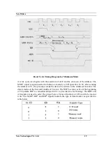
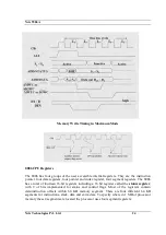
Write Cycle Timing Diagram for Minimum Mode
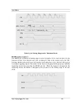
Hold Response sequence:
The HOLD pin is checked at leading edge of each clock pulse. If it is received active by the
processor before T4 of the previous cycle or during T1 state of the current cycle, the CPU
activates HLDA in the next clock cycle and for succeeding bus cycles, the bus will be given
to another requesting master. The control of the bus is not regained by the processor until the
requesting master does not drop the HOLD pin low. When the request is dropped by the
requesting master, the HLDA is dropped by the processor at the trailing edge of the next
clock.
Summary of Contents for 5586A
Page 2: ...Nvis 5586A Nvis Technologies Pvt Ltd 2...
Page 23: ...Nvis 5586A Nvis Technologies Pvt Ltd 23 Memory Read Timing in Maximum Mode...
Page 30: ...Nvis 5586A Nvis Technologies Pvt Ltd 30...
Page 48: ...Nvis 5586A Nvis Technologies Pvt Ltd 48 Diagram of module RESET power Instruction Set Note...


