Table 13. USRP-2944 Module LEDs (Continued)
LED
Description
Color
State
Indication
RF 1 TX1
RX1
Indicates the transmit
status of the module.
OFF
—
The module is not active.
Red
Solid
The module is transmitting
data.
Green
Solid
The module is receiving
data.
RX2
Indicates the receive
status of the module.
OFF
—
The module is not
receiving.
Green
Solid
The module is receiving.
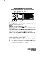
Figure 12. USRP-2944 Module Back Panel
0
1
PWR
REF
IN
PPS
OUT
TRIG
5V DC
REF
OUT
1G/10G ETH
3.3 V
+15 dBm
MAX
9-16V DC
7.5 A MAX
SFP+Ports
PCIe x4
TRIG
3.3V
IN
5V MAX
PPS
GPS
ANT
–15 dBm
MAX
Table 14. USRP-2944 Module Back Panel Connectors
Connector
Use
PWR
Input that accepts a 9 V to 16 V, 6 A external DC power connector.
1G/10G ETH
Two SFP+ input terminals used for 1G ETH or 10G ETH connectivity with
the host driver. Not currently supported in LabVIEW FPGA.
REF OUT
Output terminal for an external reference signal for the LO on the device.
REF OUT is a female SMA connector with an impedance of 50 Ω, and it is
a single-ended reference output. The output signal at this connector is
10 MHz at 3.3 V.
REF IN
Input terminal for an external reference signal for the LO on the device.
REF IN is a female SMA connector with an impedance of 50 Ω, and it is a
single-ended reference input. REF IN accepts a 10 MHz signal with a
minimum input power of 0 dBm (0.632 Vpk-pk) and a maximum input
power of 15 dBm (3.56 Vpk-pk) for a square wave or sine wave.
PCIe x4
Port for a PCI Express Generation 1, x4 bus connection through an MXI
Express four-lane cable.
26
|
ni.com
|
USRP-2940/2942/2943/2944/2945 Getting Started Guide