


2-
8
|
ni.com
Chapter 2
Using the Module
I/O Connector Signal Descriptions
Table 2-2 describes the signals found on the I/O connector.
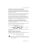
NI PXIe-4302/4303 Block Diagram
Figure 2-9 shows the block diagram of the NI PXIe-4302/4303. The analog signal conditioning
for each channel consists of a software selectable gain block and an anti-alias filter. Each
conditioned signal is then digitized by a 24-bit delta-sigma ADC to achieve simultaneous data
acquisition. After the signal is digitized it passes through various DSP steps before being sent to
software. Refer to the
Timing Engines and DSP Streams
section for more information about this
digital block.
Table 2-2.
I/O Connector Signal Descriptions
Signal Names
Direction
Description
AIGND
—
Analog Input Ground
AI<0..31>+
Input
Positive inputs of the differential analog input
channels 0 to 31.
AI<0..31>-
Input
Negative inputs of the differential analog input
channels 0 to 31.
RSVD
—
These pins are reserved for communication with the
accessory.
DGND
—
Digital ground—this pin supplies the reference for
module digital signals and is connected to the
module digital ground.
PFI0
Input
3.3 V digital signal for sending or receiving trigger
and synchronization signals. This line is referenced
to DGND.


