


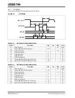

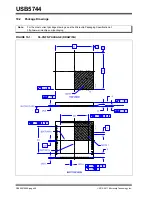

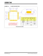


USB5744
DS00001855E-page 30
2015-2017 Microchip Technology Inc.
9.0
OPERATIONAL CHARACTERISTICS
9.1
Absolute Maximum Ratings*
+1.2 V Supply Voltage (
VDD12
) (
) . . . . . . . . . . . . . . . . . . . . . . . . . . . . . . . . . . . . . . . . . . . . . . . . -0.5 V to +1.32 V
+3.3 V Supply Voltage (
VDD33
) (
) . . . . . . . . . . . . . . . . . . . . . . . . . . . . . . . . . . . . . . . . . . . . . . . . . -0.5 V to +4.6 V
Positive voltage on input signal pins, with respect to ground (
) . . . . . . . . . . . . . . . . . . . . . . . . . . . . . . . . . . +4.6 V
Negative voltage on input signal pins, with respect to ground . . . . . . . . . . . . . . . . . . . . . . . . . . . . . . . . . . . . . . . . -0.5 V
Positive voltage on
XTALI/CLK_IN
, with respect to ground . . . . . . . . . . . . . . . . . . . . . . . . . . . . . . . . . . . . . . . . +3.63 V
Positive voltage on USB DP/DM signal pins, with respect to ground. . . . . . . . . . . . . . . . . . . . . . . . . . . . . . . . . . . +6.0 V
Positive voltage on USB 3.1 Gen 1
USB3UP_xxxx
and
USB3DN_xxxx
signal pins, with respect to ground. . . . . 1.32 V
Storage Temperature . . . . . . . . . . . . . . . . . . . . . . . . . . . . . . . . . . . . . . . . . . . . . . . . . . . . . . . . . . . . . . . -55
o
C to +150
o
C
Junction Temperature. . . . . . . . . . . . . . . . . . . . . . . . . . . . . . . . . . . . . . . . . . . . . . . . . . . . . . . . . . . . . . . . . . . . . . +125
o
C
Lead Temperature Range . . . . . . . . . . . . . . . . . . . . . . . . . . . . . . . . . . . . . . . . . . . . . Refer to JEDEC Spec. J-STD-020
HBM ESD Performance . . . . . . . . . . . . . . . . . . . . . . . . . . . . . . . . . . . . . . . . . . . . . . . . . . . . . . . . . . . . . . . . . . . . . . 3 kV
Note 1:
When powering this device from laboratory or system power supplies, it is important that the absolute max-
imum ratings not be exceeded or device failure can result. Some power supplies exhibit voltage spikes on
their outputs when AC power is switched on or off. In addition, voltage transients on the AC power line may
appear on the DC output. If this possibility exists, it is suggested to use a clamp circuit.
Note 2:
This rating does not apply to the following pins: All USB DM/DP pins,
XTAL1/CLK_IN
, and
XTALO
*Stresses exceeding those listed in this section could cause permanent damage to the device. This is a stress rating
only. Exposure to absolute maximum rating conditions for extended periods may affect device reliability. Functional
operation of the device at any condition exceeding those indicated in
Section 9.2, "Operating Conditions**"
, or any other applicable section of this specification is not implied.
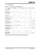
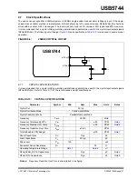
9.2
Operating Conditions**
+1.2 V Supply Voltage (
VDD12
) . . . . . . . . . . . . . . . . . . . . . . . . . . . . . . . . . . . . . . . . . . . . . . . . . . . . . +1.08 V to +1.32 V
+3.3 V Supply Voltage (
VDD33
) . . . . . . . . . . . . . . . . . . . . . . . . . . . . . . . . . . . . . . . . . . . . . . . . . . . . . . . +3.0 V to +3.6 V
Input Signal Pins Voltage (
) . . . . . . . . . . . . . . . . . . . . . . . . . . . . . . . . . . . . . . . . . . . . . . . . . . . . . . -0.3 V to +3.6 V
XTALI/CLK_IN
Voltage. . . . . . . . . . . . . . . . . . . . . . . . . . . . . . . . . . . . . . . . . . . . . . . . . . . . . . . . . . . . . . -0.3 V to +3.6 V
USB 2.0 DP/DM Signal Pins Voltage . . . . . . . . . . . . . . . . . . . . . . . . . . . . . . . . . . . . . . . . . . . . . . . . . . . . -0.3 V to +5.5 V
USB 3.1 Gen 1
USB3UP_xxxx
and
USB3DN_xxxx
Signal Pins Voltage . . . . . . . . . . . . . . . . . . . . . . . . -0.3 V to +1.32 V
Ambient Operating Temperature in Still Air (T
A
) . . . . . . . . . . . . . . . . . . . . . . . . . . . . . . . . . . . . . . . . . . . . . . . . . . .
+1.2 V Supply Voltage Rise Time (T
RT
in
) . . . . . . . . . . . . . . . . . . . . . . . . . . . . . . . . . . . . . . . . . . . . . . 400 µs
+3.3 V Supply Voltage Rise Time (T
RT
) . . . . . . . . . . . . . . . . . . . . . . . . . . . . . . . . . . . . . . . . . . . . . . 400 µs
Note 3:
0
o
C to +70
o
C for commercial version, -40
o
C to +85
o
C for industrial version.
**Proper operation of the device is guaranteed only within the ranges specified in this section.
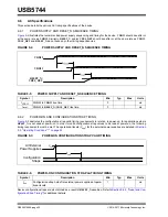
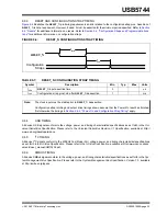
Note:
Do not drive input signals without power supplied to the device.


