background image

6.1.1. Forcible Disc Eject

6.1.1.1. When the power can be turned off.

1. Turn off the power and press [STOP] [CH UP] keys on the front panel 

simultaneously for 5 seconds.

6.1.1.2. When the power can not be turned off.

1. Press [POWER] key on the front panel for over 10 seconds to turn off 

the power forcibly, and press [STOP] [CH UP] keys on the front panel 
simultaneously for 5 seconds.

6.1.2. When the Forcible Disc Eject can not be done.

1. Turn off the power and pull out AC cord.

2. Remove the Top Case.

3. Put deck so that bottom can be seen.

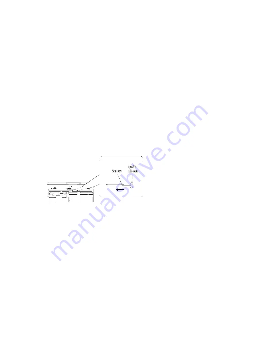
4. Slide SLIDE CAM by Eject Pin (JZJ0484) or minus screw driver (small) 

in the direction of arrow to eject tray slightly.

5. Put deck upward, and push out Tray by Eject Pin (JZS0484) or minus 

screw driver (small).

10

Summary of Contents for DMR-ES15PL

Page 1: ...ORDER NO CHM0606039CE DVD Recorder DMR ES15PL Vol 1 Colour S Silver Type SPECIFICATIONS 2006 Matsushita Electric Industrial Co Ltd All rights reserved 1...

Page 2: ...nt the customer from being exposed to shock hazards 1 1 1 Leakage current cold check 1 Unplug the AC cord and connect a jumper between the two prongs on the plug 2 Measure the resistance value with an...

Page 3: ...Electrostatic Sensitive ES Devices Some semiconductor solid state devices can be damaged easily by static electricity Such components commonly are called Electrostatic Sensitive ES Devices Examples of...

Page 4: ...minum foil or comparable conductive material 7 Immediately before removing the protective material from the leads of a replacement ES device touch the protective material to the chassis or circuit ass...

Page 5: ...Ag and Copper Cu and the melting point of the lead free solder is higher approx 30 degrees C 86 F more than that of the normal solder Definition of PCB Lead Free Solder being used The letter of PbF is...

Page 6: ...eplace the Lithium Battery REPLACEMENT PROCEDURE 1 Remove the Top case Front Panel RAM Digital P C B Module DV Jack Rear Panel Front L P C B and Main P C B by referring the Disassembling Procedure 2 U...

Page 7: ...3 Service Navigation 3 1 Service Information 4 Specifications 7...

Page 8: ...5 Location of Controls and Components 8...

Page 9: ...6 Operation Instructions 6 1 Taking out the Disc from DVD Drive Unit when the Disc cannot be ejected by OPEN CLOSE button 9...

Page 10: ...to turn off the power forcibly and press STOP CH UP keys on the front panel simultaneously for 5 seconds 6 1 2 When the Forcible Disc Eject can not be done 1 Turn off the power and pull out AC cord 2...

Page 11: ...Diagnosis contents Description Monitor Display Automatic FL display U30 Remote control code error Display appears when main unit and remote controller codes are not matched No display is remote contr...

Page 12: ...up for program recording When initialization error is detected after starting up main microprocessor for program recording the power is turned off automatically The event is saved in memory No displa...

Page 13: ...ase Quick Start of setup menu is ON it is displayed in restoration operation for AC off No display UNFORMAT Unformatted disc error You have inserted an unformatted DVD RAM or DVD RW that is unformatte...

Page 14: ...effective during Child lock is ON While Demonstration Lock is being set this Forced disc eject function is not accepted The display before execution leaves When the power is off press STOP and CH key...

Page 15: ...usly for over seconds and less than seconds NOTE1 If Unit has not turned into Aging mode by operations shown above execute TEST MODE once and execute operation shown above All the main unit s paramete...

Page 16: ...ously for 5 seconds When press OPEN CLOSE key while the tray being locked Display LOCK for 3 seconds Press OPEN CLOSE key while the tray being locked ATP Initialization ATP setting is initialized and...

Page 17: ...5 ROM correction version left displayed are version displays Press 0 2 in service mode White Picture Output White picture is output as component Output from AV Decoder White picture Saturation rate 10...

Page 18: ...modes Initial mode is Interlace Switch Interlace Progressive Press 1 4 in I P Switch mode I P are switched alternately Audio Mute XTMUTE Check whether mute is applied normally by the timer microproce...

Page 19: ...is displayed for 5 seconds 2 Time when the error has occurred is displayed for 5 seconds DD Day hh Hour mm Minute 3 Last Drive Error 1 2 is displayed for 5 seconds 4 Last Drive Error 2 2 is displayed...

Page 20: ...nd all LEDs are turned on All segments are turned on Press 5 1 in service mode S1 signal output Forcibly superimpose the S1 signal approx 4 5V DC on the EE chroma signal and check the output on the S...

Page 21: ...B AV DEC MAIN CPU 02 Defect of RAM Drive 03 Defect of Disc 04 Defect of Digital P C B or Communication Error 05 Defect of Digital P C B AV DEC MAIN CPU 06 Defect of HDD Display the time when the error...

Page 22: ...rvice Mode Display in STOP E E mode Press power button on front panel or Remote controller in service mode 8 Service Fixture Tools Part Number Description Compatibility RFKZ0365 Extension Cable MainP...

Page 23: ...B Positions 9 3 Top Case 1 Remove the 2 screws A and 3 screws B 2 Slide Top Case rearward and open the both ends at rear side of the Top Case a little and lift the Top Case in the direction of the ar...

Page 24: ...9 4 Front Panel 1 Unlock 6 tabs in A F turn Pull with the front panel in the direction of your side 9 5 RAM Digital P C B Module 24...

Page 25: ...1 Remove 6 Screws A 2 Lift up Digital P C B slightly so to disconnect Connectors to remove Digital P C B 3 Put Digital P C B on RAM Drive and remove RAM Digital P C B Module 25...

Page 26: ...AM Digital P C B Module as service part has no heat sink unit Before returning to customer heat sink unit should be installed on Digital P C B 9 6 DV Jack P C B 1 Remove a Screw A to remove DV jack P...

Page 27: ...ove 1 Screw A 2 Front L P C B is removed in the direction of the arrow 3 Unsolder soldering of wire and remove Front L P C B 9 8 Rear Panel 1 Remove 6 Screws A and 1 Screw B 2 Unlock 2 Locking Tabs A...

Page 28: ...9 9 Power P C B 1 Remove 1 Screw A 2 Remove 3 Screws B and disconnect conector A to remove Power P C B 28...

Page 29: ...9 10 Main P C B 1 Remove 8 Screws A and 1 Screw B 2 Remove Digital Angle to remove Main P C B 10 Measurements and Adjustments 10 1 Service Positions 29...

Page 30: ...Note For description of the disassembling procedure see the section 9 10 1 1 Checking and Repairing Power P C B 10 1 2 Checking and Repairing of RAM Digital P C B Module 30...

Page 31: ...10 1 3 Checking and Repairing of Main P C B 31...

Page 32: ...Digital P C B Module Once power off and start up again 10 3 When the unit does not operate normally after replacing the Timer Microprocessor or Main P C B When the unit does not operate normally after...

Page 33: ...ntarily RESET L is transmitted to the X REST of Timer Microprocessor IC7501 8 pin then the unit operates normally 10 4 Standard Inspection Specifications after Making Repairs 11 Block Diagram 11 1 Pow...

Page 34: ...agram A 12 8 Timer 1 4 Section Main P C B 3 3 Schematic Diagram FL 12 9 Timer 2 4 Section Main P C B 3 3 Schematic Diagram FL 12 10 Timer 3 4 Section Main P C B 3 3 Schematic Diagram FL 12 11 Timer 4...

Page 35: ...information when probing defect point because it may differ from an actual measuring value due to difference of Measuring instrument and its measuring condition and product itself 14 1 1 Power P C B 1...

Page 36: ...OUT CONSTANT ANGULAR VELOCITY CAP BLACK DROP OUT COMPACT DISC CD SERIAL DATA CLOCK CD SERIAL DATA CD RF EFM SIGNAL COMPACT DISC VIDEO CHANNEL DATA SYSTEM CLOCK SELECT CONSTANT LINEAR VELOCITY CAP OFF...

Page 37: ...REFERENCE INTERFACE MODE SELECT L LDON LPC LRCK LASER DIODE CONTROL LASER POWER CONTROL L CH R CH DISTINCTION CLOCK M MA0 UP MCK MCKI MCLK MDATA MDQ0 UP MDQM MLD MPEG MEMORY ADDRESS MEMORY CLOCK MEMOR...

Page 38: ...T CLOCK SERIAL PORT ENABLE SERIAL DATA IN SERIAL DATA OUT SERIAL PORT DATA INPUT SERIAL PORT DATA OUTPUT SERIAL PORT R W ENABLE SERIAL PORT READ CLOCK SERIAL PORT WRITE CLOCK SUB CODE Q CLOCK SUB CODE...

Page 39: ...S XHSYNCO XHINT XI XINT XMW XO XRE XSRMCE XSRMOE XSRMWE XVCS XVDS XVSYNCO X TAL X ADDRESS LATCH ENABLE X AUDIO DATA REQUEST X CD ROM CHIP SELECT X CHIP SELECT X COMPOSITE SYNC X DATA STROBE X HORIZONT...

Page 40: ...15 1 2 Packing Accessories Section 40...

Page 41: ...of components be sure to use only manufactures specified parts shown in the parts list Warning This product uses a laser diode Refer to caution statements Capacity values are in microfarads F unless...

Page 42: ...680P 1 C1513 F1J0J106A014 6 3V 10U 1 C1518 F1H1A105A028 10V 1U 1 C1519 F2A1A470A388 10V 47U 1 C1521 F1H1A105A028 10V 1U 1 C1522 F1H1A105A028 10V 1U 1 C1523 F2A1A470A388 10V 47U 1 C1524 F2A1A101A389 1...

Page 43: ...3901 ECJ1VB1H103K 50V 0 01U 1 C3902 ECJ1VB1H103K 50V 0 01U 1 C3903 ECJ1VB1C104K 16V 0 1U 1 C3904 ECJ1VB1C104K 16V 0 1U 1 C3905 ECJ1VB1H103K 50V 0 01U 1 C3907 ECJ1VB1C104K 16V 0 1U 1 C3908 ECJ1VB1H103K...

Page 44: ...C4030 ECJ1VC1H102J 50V 1000P 1 44...

Page 45: ...20 50V 10P 1 C7525 ECJ1VF1A105Z 10V 1U 1 C7527 F2A1C221A877 16V 220P 1 C7530 F2A1C221A877 16V 220P 1 C7531 ECQB1H392KF3 50V 3900P 1 C7532 F2A1V470A654 35V 47P 1 C7533 F2A1H100A820 50V 10P 1 C7534 ECJ1...

Page 46: ...D7502 MA2C165001VT DIODE 1 46...

Page 47: ...04 C0BBBB000014 IC 1 IC7501 MN67789RA IC 1 IC7502 C0EBE0000194 IC 1 IC7514 C0EBJ0000336 IC 1 IP1501 K5H302100004 IC PROTECTOR 1 IP7501 K5H7512A0010 IC PROTECTOR 1 IR7501 PNA4618M09VT REMOTE SENSOR 1 J...

Page 48: ...48...

Page 49: ...J0JHC0000048 FILTER 1 LB7501 ERJ3GEY0R00V 1 10W 0 1 LB7503 ERJ3GEY0R00V 1 10W 0 1 LB7504 ERJ3GEY0R00V 1 10W 0 1 LB7801 J0JHC0000032 COIL 1 LB7802 J0JHC0000032 COIL 1 LB8001 ERJ3GEY0R00V 1 10W 0 1 P150...

Page 50: ...QR7502 UNR521200L TRANSISTOR 1 50...

Page 51: ...75 1 R3903 ERJ3GEYJ102V 1 10W 1K 1 R3904 ERJ3GEYJ102V 1 10W 1K 1 R3905 ERJ3GEYJ750V 1 10W 75 1 R3906 ERJ3GEYJ750V 1 10W 75 1 R3907 ERJ3GEYJ750V 1 10W 75 1 R3908 ERJ3GEYJ750V 1 10W 75 1 R3909 ERJ3GEYJ...

Page 52: ...R4017 D0HB561ZA002 1 10W 560 1 52...

Page 53: ...1 10W 4 7K 1 R7404 ERJ3GEY0R00V 1 10W 0 1 R7406 ERJ3GEYJ472V 1 10W 4 7K 1 R7439 ERJ3GEYJ223V 1 10W 22K 1 R7501 ERJ3GEYJ473V 1 10W 47K 1 R7502 ERJ3GEYJ473V 1 10W 47K 1 R7504 ERJ3GEY0R00V 1 10W 0 1 R75...

Page 54: ...R7536 ERJ3GEYJ473V 1 10W 47K 1 54...

Page 55: ...575 ERJ3GEYJ473V 1 10W 47K 1 R7576 ERJ3GEYJ101V 1 10W 100 1 R7582 ERJ3GEYJ473V 1 10W 47K 1 R7584 ERJ3GEYJ101V 1 10W 100 1 R7585 ERJ3GEYJ473V 1 10W 47K 1 R7586 ERJ3GEYJ473V 1 10W 47K 1 R7587 ERJ3GEYJ47...

Page 56: ...S7507 EVQ11A04M SWITCH 1 56...

Page 57: ...1 8W 0 1 W521 ERJ6GEY0R00V 1 8W 0 1 W522 ERJ3GEY0R00V 1 10W 0 1 W523 ERJ3GEY0R00V 1 10W 0 1 W524 ERJ6GEY0R00V 1 8W 0 1 W525 ERJ6GEY0R00V 1 8W 0 1 W526 ERJ3GEY0R00V 1 10W 0 1 W527 ERJ3GEY0R00V 1 10W 0...

Page 58: ...MQ1566 GASKET 2 28 RFKNES15PL RAM DIGITAL P C B MODULE 1 RTL 29 VKC0295 RIVET 2 A1 EUR7659Y10 REMOTE CONTROL ASS Y 1 A1 1 UR76EC5903A BATTERY COVER 1 A2 K2CQ2CA00002 AC CORD 1 A3 K2KA6BA00003 AV CORD...

Page 59: ...55 REC PLAY 0 5Vp p 20 sec div P7401 51 REC PLAY 1 0Vp p 20 sec div P7401 39 REC PLAY 1 0Vp p 20 sec div P7401 17 19 REC PLAY 0 8Vp p 1m sec div P7401 47 REC PLAY 0 5Vp p 20 sec div JK3903 3 REC PLAY...

Page 60: ...4 PLAY 50 7 0 2 0 17 2 0 3 0 10 3 2 4 STOP 50 7 0 2 0 17 2 0 3 0 10 3 2 4 Ref No MODE 1 2 3 4 5 6 7 8 9 10 11 12 13 14 15 16 REC 0 0 5 4 3 4 2 6 12 0 9 3 0 9 0 9 0 PLAY 0 0 5 4 3 4 2 6 12 0 9 3 0 9 0...

Page 61: ...0 3 3 0 3 3 0 3 3 2 5 2 5 3 2 0 1 7 0 0 0 3 3 0 3 3 1 1 PLAY 0 3 3 0 3 3 0 3 3 2 5 2 5 3 2 0 1 7 0 0 0 3 3 0 3 3 1 1 STOP 0 3 3 0 3 3 0 3 3 2 5 2 5 3 2 0 1 7 0 0 0 3 3 0 3 3 1 1 Ref No MODE 41 42 43 4...

Page 62: ...18 1 17 7 17 7 17 7 17 7 21 1 21 1 14 3 17 6 17 6 17 6 14 2 14 2 21 0 21 0 10 8 17 6 Ref No MODE 61 62 63 64 65 66 67 68 69 70 71 72 73 74 75 76 77 78 79 80 REC 17 6 17 6 17 6 17 9 4 9 0 2 0 4 0 0 0 P...

Page 63: ...1 2 7 0 1 8 4 9 Ref No MODE 21 22 23 24 25 26 27 28 29 30 31 32 33 34 35 36 37 38 39 40 REC 1 4 0 0 1 2 7 4 9 1 7 1 8 1 9 1 9 2 2 0 2 2 2 2 2 2 2 2 1 7 1 7 0 1 8 5 0 PLAY 1 4 0 0 1 2 7 4 9 1 7 1 8 1...

Page 64: ...47 ANA5V CPNCIN DM D1 2V DGND D1 2V V YIN DM D1 2V DGND D1 2V BPBOUT DM D1 2V DGND D1 2V GPYOUT DM D3 8V DGND D3 8V RPROUT DM EPG ON H BUSY DGND ANA3 3V COUT DM CSYNC IN DGND P OFF L3 YOUT DM UARTM2P...

Page 65: ...47 ANA5V CPNCIN DM D1 2V DGND D1 2V V YIN DM D1 2V DGND D1 2V BPBOUT DM D1 2V DGND D1 2V GPYOUT DM D3 8V DGND D3 8V RPROUT DM EPG ON H BUSY DGND ANA3 3V COUT DM CSYNC IN DGND P OFF L3 YOUT DM UARTM2P...

Page 66: ...V PC001 FAN GND FANLOCK D3 8V D3 8V D3 8V X SW 12V X SW 12V X SW 12V X SW 12V GND GND GND GND X SW5 8V X SW5 8V X SW5 8V X SW5 8V 23 22 21 20 19 18 17 16 15 14 13 12 11 10 9 8 7 6 5 4 3 2 1 ST3D200 D0...

Page 67: ...V PC001 FAN GND FANLOCK D3 8V D3 8V D3 8V X SW 12V X SW 12V X SW 12V X SW 12V GND GND GND GND X SW5 8V X SW5 8V X SW5 8V X SW5 8V 23 22 21 20 19 18 17 16 15 14 13 12 11 10 9 8 7 6 5 4 3 2 1 ST3D200 D0...

Page 68: ...8 R1510 1500 D 0 01 C1511 1 2 C1521 10V F1H1A105A028 2 4 3 5 1 2 4 1 3 5 C0DAEYH00002 IC1506 1 2 K1501 VWJ0795 5 C1509 F1H1A105A028 DDGND JC_P_ON_H GND DR_GND P_OFF_L 6 5 2 4 3 7 1 4 5 6 7 2 1 3 IC150...

Page 69: ...8 R1510 1500 D 0 01 C1511 1 2 C1521 10V F1H1A105A028 2 4 3 5 1 2 4 1 3 5 C0DAEYH00002 IC1506 1 2 K1501 VWJ0795 5 C1509 F1H1A105A028 DDGND JC_P_ON_H GND DR_GND P_OFF_L 6 5 2 4 3 7 1 4 5 6 7 2 1 3 IC150...

Page 70: ...25 1 2 R4026 D0HB622ZA002 1 2 R4028 D0HB392ZA002 1 2 LB7406 0 1 2 L7401 VWJ0795 1 2 R4017 D0HB561ZA002 1 2 R4018 D0HB153ZA002 1 2 R4016 D0HB561ZA002 1 2 100 R4013 2 1 C4012 16V220 1 2 100 R4014 1 2 R4...

Page 71: ...25 1 2 R4026 D0HB622ZA002 1 2 R4028 D0HB392ZA002 1 2 LB7406 0 1 2 L7401 VWJ0795 1 2 R4017 D0HB561ZA002 1 2 R4018 D0HB153ZA002 1 2 R4016 D0HB561ZA002 1 2 100 R4013 2 1 C4012 16V220 1 2 100 R4014 1 2 R4...

Page 72: ...2 75 R3908 11 7 9 8 1 3 5 13 4 12 15 20 18 19 21 16 17 14 2 6 10 JK3901 K2HE110B0001 1 2 50V ECQV1H104JL3 C4033 1 2 16V 0 1 ZF C4035 1 2 50V C4036 ECQV1H104JL3 1 2 16V 0 1 ZF C4034 20 18 21 17 K2HE109...

Page 73: ...2 75 R3908 11 7 9 8 1 3 5 13 4 12 15 20 18 19 21 16 17 14 2 6 10 JK3901 K2HE110B0001 1 2 50V ECQV1H104JL3 C4033 1 2 16V 0 1 ZF C4035 1 2 50V C4036 ECQV1H104JL3 1 2 16V 0 1 ZF C4034 20 18 21 17 K2HE109...

Page 74: ...1YYB0002 1 2 LB3912 0 1 2 LB3911 0 L S C V Y R T A B C D E F G I J K L M N O P Q R S 1 2 3 4 5 6 7 8 9 10 11 12 13 14 15 19 20 21 22 23 24 25 5 4 3 2 1 C B A B TO A V I O SECTION 1 4 DMR ES15PL A V I...

Page 75: ...1YYB0002 1 2 LB3912 0 1 2 LB3911 0 L S C V Y R T A B C D E F G I J K L M N O P Q R S 1 2 3 4 5 6 7 8 9 10 11 12 13 14 15 19 20 21 22 23 24 25 5 4 3 2 1 C B A B TO A V I O SECTION 1 4 DMR ES15PL A V I...

Page 76: ...13 12 11 14 37 9 7 5 3 1 2 4 6 8 10 39 IC3001 C1AB00001979 1 2 16V C3014 0 1 1 2 C3013 16V47 CPN OUT2 LINE OUT V2 C Y T C 2 IN S1 S2 DET2 SW GND2 C S DET3 VIDEO 3 IN DGND1 C S DET2 Y 2 IN C 1 IN VIDE...

Page 77: ...13 12 11 14 37 9 7 5 3 1 2 4 6 8 10 39 IC3001 C1AB00001979 1 2 16V C3014 0 1 1 2 C3013 16V47 CPN OUT2 LINE OUT V2 C Y T C 2 IN S1 S2 DET2 SW GND2 C S DET3 VIDEO 3 IN DGND1 C S DET2 Y 2 IN C 1 IN VIDE...

Page 78: ...C S DET2 6 13 10 BIAS C3 IN 17 5 7 CLAMP Y3 IN 14 21 24 19 CLAMP VIDEO3 IN 12 3 35 43 51 33 47 36 37 39 27 26 29 28 30 41 27 24 OUTR RFOUT 26 DAL DAR 25 0 5dB 0 5dB SELECTOR INPUT 6 1dB 6 1dB 2 LOGIC...

Page 79: ...C S DET2 6 13 10 BIAS C3 IN 17 5 7 CLAMP Y3 IN 14 21 24 19 CLAMP VIDEO3 IN 12 3 35 43 51 33 47 36 37 39 27 26 29 28 30 41 27 24 OUTR RFOUT 26 DAL DAR 25 0 5dB 0 5dB SELECTOR INPUT 6 1dB 6 1dB 2 LOGIC...

Page 80: ...1 20 22 41 24 39 37 33 35 34 29 30 27 26 28 32 31 36 38 25 40 42 44 13 46 IC7501 MN67789RA 1 2 R7513 4700 AFC_T 1 2 R7584 100 1 2 50V 100P C7521 1 2 10V C7523 F1H1A105A028 SBPTM_T P_OFF_L SBMTP_T JC_P...

Page 81: ...1 20 22 41 24 39 37 33 35 34 29 30 27 26 28 32 31 36 38 25 40 42 44 13 46 IC7501 MN67789RA 1 2 R7513 4700 AFC_T 1 2 R7584 100 1 2 50V 100P C7521 1 2 10V C7523 F1H1A105A028 SBPTM_T P_OFF_L SBMTP_T JC_P...

Page 82: ...545 2 3 1 Q7501 2SD132800L 1 2 R7543 10K HDMI_MONI 1 2 R7558 10K 1 2 16V C7516 0 1 1 2 B7501 CR2354 1GUF N4BCT50A0005 2 1 C7538 F2A0J471A574 1 2 R7560 1K 1 2 D7509 B0JACE000001 1 2 TW7501 VWJ0795 12 5...

Page 83: ...545 2 3 1 Q7501 2SD132800L 1 2 R7543 10K HDMI_MONI 1 2 R7558 10K 1 2 16V C7516 0 1 1 2 B7501 CR2354 1GUF N4BCT50A0005 2 1 C7538 F2A0J471A574 1 2 R7560 1K 1 2 D7509 B0JACE000001 1 2 TW7501 VWJ0795 12 5...

Page 84: ...2 50V C7512 24P 1 2 50V 27P C7513 1 2 3 2 1 3 1 2 X7503 EFOMC1005T4 H2B100500007 1 2 R7505 ERJ3GEY0R00V 1 2 X7502 1 2 ERJ3GEY0R00V R7504 1 2 270K R7573 A CH_UP CH_DOWN OPEN CLOSE PLAY STOP NC GND KEY...

Page 85: ...2 50V C7512 24P 1 2 50V 27P C7513 1 2 3 2 1 3 1 2 X7503 EFOMC1005T4 H2B100500007 1 2 R7505 ERJ3GEY0R00V 1 2 X7502 1 2 ERJ3GEY0R00V R7504 1 2 270K R7573 A CH_UP CH_DOWN OPEN CLOSE PLAY STOP NC GND KEY...

Page 86: ...T_PLUG R7561 0 AG NOTE DO NOT USE THE PART NUMBER SHOWN ON THIS DRAWING FOR ORDERRING THE CORRECT PART NUMBER IS SHOWN IN THE PARTS LIST AND MAY BE SLIGHTLYDIFFERNT OR AMENDED SINCE THIS DRAWING WAS P...

Page 87: ...T_PLUG R7561 0 AG NOTE DO NOT USE THE PART NUMBER SHOWN ON THIS DRAWING FOR ORDERRING THE CORRECT PART NUMBER IS SHOWN IN THE PARTS LIST AND MAY BE SLIGHTLYDIFFERNT OR AMENDED SINCE THIS DRAWING WAS P...

Page 88: ...6 47 48 75 49 64 XT MUTE 100 JC P ON H 7 DIP ON H 23 P SAVE H P FAL L 29 IR 25 32KHz OUT 14 32KHz IN 13 GND VDD OUT 1 3 2 Vref GND VDD OUT 1 3 2 Vref 8 7 6 5 1 2 3 4 B IN B IN BOUT V GND A IN A IN AOU...

Page 89: ...6 47 48 75 49 64 XT MUTE 100 JC P ON H 7 DIP ON H 23 P SAVE H P FAL L 29 IR 25 32KHz OUT 14 32KHz IN 13 GND VDD OUT 1 3 2 Vref GND VDD OUT 1 3 2 Vref 8 7 6 5 1 2 3 4 B IN B IN BOUT V GND A IN A IN AOU...

Page 90: ...LYDIFFERNT OR AMENDED SINCE THIS DRAWING WAS PREPARED 12 13 DV Jack Schematic Diagram 2 1 4 3 P37002 K2HZ104B0012 2 4 3 1 6 5 K1KA06B00181 P37001 TO PS57001 DIGITAL P C B BE 2 4 SECTION TO DV JACK TPB...

Page 91: ...LYDIFFERNT OR AMENDED SINCE THIS DRAWING WAS PREPARED 12 13 DV Jack Schematic Diagram 2 1 4 3 P37002 K2HZ104B0012 2 4 3 1 6 5 K1KA06B00181 P37001 TO PS57001 DIGITAL P C B BE 2 4 SECTION TO DV JACK TPB...

Page 92: ...USE THE PART NUMBER SHOWN ON THIS DRAWING FOR ORDERRING THE CORRECT PART NUMBER IS SHOWN IN THE PARTS LIST AND MAY BE SLIGHTLYDIFFERNT OR AMENDED SINCE THIS DRAWING WAS PREPARED 10 9 8 7 6 C TO TIMER...

Page 93: ...C7513 1 2 3 2 1 3 1 2 X7503 EFOMC1005T4 H2B100500007 1 2 R7505 ERJ3GEY0R00V 1 2 X7502 1 2 ERJ3GEY0R00V R7504 1 2 270K R7573 A CH_UP CH_DOWN OPEN CLOSE PLAY STOP NC GND KEY13_POWER GND REC or A A A A...

Page 94: ...2 R7543 10K HDMI_MONI 1 2 R7558 10K 1 2 16V C7516 0 1 1 2 B7501 CR2354 1GUF N4BCT50A0005 2 1 C7538 F2A0J471A574 1 2 R7560 1K 1 2 D7509 B0JACE000001 1 2 TW7501 VWJ0795 12 5 1 2 R7599 47K HDMI_P5_ON_H...

Page 95: ...29 30 27 26 28 32 31 36 38 25 40 42 44 13 46 IC7501 MN67789RA 1 2 R7513 4700 AFC_T 1 2 R7584 100 1 2 50V 100P C7521 1 2 10V C7523 F1H1A105A028 SBPTM_T P_OFF_L SBMTP_T JC_P_ON_H SCLK_T FANLOCK A P A A...

Page 96: ...2 C1521 10V F1H1A105A028 2 4 3 5 1 2 4 1 3 5 C0DAEYH00002 IC1506 1 2 K1501 VWJ0795 5 C1509 F1H1A105A028 DDGND JC_P_ON_H GND DR_GND P_OFF_L 6 5 2 4 3 7 1 4 5 6 7 2 1 3 IC1504 C0DBGHF00001 D3R8V JC_REG5...

Page 97: ...D3 8V D3 8V D3 8V X SW 12V X SW 12V X SW 12V X SW 12V GND GND GND GND X SW5 8V X SW5 8V X SW5 8V X SW5 8V 23 22 21 20 19 18 17 16 15 14 13 12 11 10 9 8 7 6 5 4 3 2 1 ST3D200 D005 STRG6353 IC001 1 4 3...

Page 98: ...D1 2V V YIN DM D1 2V DGND D1 2V BPBOUT DM D1 2V DGND D1 2V GPYOUT DM D3 8V DGND D3 8V RPROUT DM EPG ON H BUSY DGND ANA3 3V COUT DM CSYNC IN DGND P OFF L3 YOUT DM UARTM2P DGND UARTP2M DGND DGND DGND I...

Page 99: ...46 47 48 75 49 64 XT MUTE 100 JC P ON H 7 DIP ON H 23 P SAVE H P FAL L 29 IR 25 32KHz OUT 14 32KHz IN 13 GND VDD OUT 1 3 2 Vref GND VDD OUT 1 3 2 Vref 8 7 6 5 1 2 3 4 B IN B IN BOUT V GND A IN A IN A...

Page 100: ...0 C S DET2 6 13 10 BIAS C3 IN 17 5 7 CLAMP Y3 IN 14 21 24 19 CLAMP VIDEO3 IN 12 3 35 43 51 33 47 36 37 39 27 26 29 28 30 41 27 24 OUTR RFOUT 26 DAL DAR 25 0 5dB 0 5dB SELECTOR INPUT 6 1dB 6 1dB 2 LOGI...

Page 101: ...GND NC GND KEY3_POWER POWER B 4 3 2 1 A DMR ES15PL Front L Schematic Diagram NOTE DO NOT USE THE PART NUMBER SHOWN ON THIS DRAWING FOR ORDERRING THE CORRECT PART NUMBER IS SHOWN IN THE PARTS LIST AND...

Page 102: ...PB TPA TPA IMSA 9390S 04Z901 TPB TPB TPB TPA NC NC TPA IMSA 9850B 06Z900 B 4 3 2 1 A DMR ES15PL DV Jack Schematic Diagram NOTE DO NOT USE THE PART NUMBER SHOWN ON THIS DRAWING FOR ORDERRING THE CORREC...

Page 103: ...6 8 10 39 IC3001 C1AB00001979 1 2 16V C3014 0 1 1 2 C3013 16V47 CPN OUT2 LINE OUT V2 C Y T C 2 IN S1 S2 DET2 SW GND2 C S DET3 VIDEO 3 IN DGND1 C S DET2 Y 2 IN C 1 IN VIDEO 2 IN ADR V75 OUT C75 OUT DV...

Page 104: ...3911 0 L S C V Y R T A B C D E F G I J K L M N O P Q R S 1 2 3 4 5 6 7 8 9 10 11 12 13 14 15 19 20 21 22 23 24 25 5 4 3 2 1 C B A B TO A V I O SECTION 1 4 DMR ES15PL A V I O 3 4 Section Main P C B 2 3...

Page 105: ...4 12 15 20 18 19 21 16 17 14 2 6 10 JK3901 K2HE110B0001 1 2 50V ECQV1H104JL3 C4033 1 2 16V 0 1 ZF C4035 1 2 50V C4036 ECQV1H104JL3 1 2 16V 0 1 ZF C4034 20 18 21 17 K2HE109B0001 JK3902 2 1 6V470 C4031...

Page 106: ...R4028 D0HB392ZA002 1 2 LB7406 0 1 2 L7401 VWJ0795 1 2 R4017 D0HB561ZA002 1 2 R4018 D0HB153ZA002 1 2 R4016 D0HB561ZA002 1 2 100 R4013 2 1 C4012 16V220 1 2 100 R4014 1 2 R4015 D0HB153ZA002 1 2 R4021 D0...

Page 107: ...M2C Z002 C 6 Capacitor C105 B 2 R006 C 5 R119 C 2 IC001 B 4 ZD002 C 5 C001 C 6 C106 B 3 R007 C 5 R120 B 2 IC101 B 3 ZD004 B 4 C002 B 6 C107 B 2 R008 B 5 R121 B 2 IC102 C 2 ZD101 C 2 C003 B 6 C108 B 2...

Page 108: ...1509 C 3 R4021 E 6 R7546 F 3 Battery Q7511 E 4 CL8020 A 7 LB3915 B 2 C3016 B 7 C4026 E 7 R1510 C 3 R4022 E 6 R7548 F 3 B7501 E 5 Q7513 E 4 TL7401 D 5 LB3916 B 3 C3017 C 6 C4029 E 7 R1511 D 3 R4023 D 7...

Page 109: ...Location Map REAR DMR ES15PL Main P C B RFKB79116D 4 4 Section 1 4 2 4 3 4 4 4 FRONT...

Page 110: ...D E F Main P C B Location Map REAR DMR ES15PL Main P C B RFKB79116D 3 4 Section 1 4 2 4 3 4 4 4 FRONT...

Page 111: ...5 6 7 8 Location Map REAR DMR ES15PL Main P C B RFKB79116D 2 4 Section 1 4 2 4 3 4 4 4 FRONT...

Page 112: ...1 2 3 4 A B C Location Map REAR DMR ES15PL Main P C B RFKB79116D 1 4 Section 1 4 2 4 3 4 4 4 FRONT...

Page 113: ...1 2 3 4 5 6 7 8 A B C D DMR ES15PL DV Jack P C B VEP73135A DV Jack P C B...

Page 114: ...1 2 3 4 5 6 7 8 A B DMR ES15PL Front L P C B VEP70135A Front L P C B...

Page 115: ...P7401 P59001 D 1 2V 52 54 56 58 60 62 P59001 P7401 POWER OFF 18 P59001 P7401 30 8 IC7501 ON 1 5 ON ON ON 13 IC4001 VOUT VIN 5 1 4 REG AU 9V IC4003 IC7401 8 8 VIN IC1502 1 REG XSW 5 2V VOUT DMR ES15PL...

Page 116: ...OLD HOT SWITCHING IC IC001 VCC GND DRAIN Z C 1 4 5 RECTIFIER C009 D001 L001 L002 Z001 Z002 ABSORBER SURGE AND SUPPRESSOR SURGE F001 P001 AC SOCKET DMR ES15PL Power Supply Block Diagram D102 D101 D006...

Page 117: ...59001 P59001 58 57 34 32 L123 SWIDE BLOCK SECTION TO DIGITAL Y V OUT A COUT A 65 69 59 P59001 P7401 V YIN DM 63 P59001 P7401 CPNCIN DM RPC R OUT BPC B OUT GPC Y OUT CPN Y OUT CPS V OUT CPN C OUT C S D...

Page 118: ...XSW 5 2V SEG1 64 49 SEG16 48 42 DIG7 DIG1 P SAVE XC OUT XC IN 14 13 REAL TIME CLK 32 768KHz X7502 BATTERY BACK UP B7501 9 X SW 5 2V PLAY S7502 SELECT S7507 CH UP S7504 IC7501 TIMER DISPLAY DRIVE FRONT...

Page 119: ...001 17 P7401 28 29 IIC DATA IIC CLOCK P59001 24 P7401 P59001 26 P7401 OPTICAL 1 DIGITAL AUDIO OUT IC4901 SECTION DIGITAL BLOCK FROM 32 P59001 P7401 IECOUT MIX L OUT2 MIX R OUT2 17 20 LINE OUT2 L OUT2...

Reviews: