background image

29

2.  Updating by DPMS

Download the latest firmware from the internet and update the firmware.

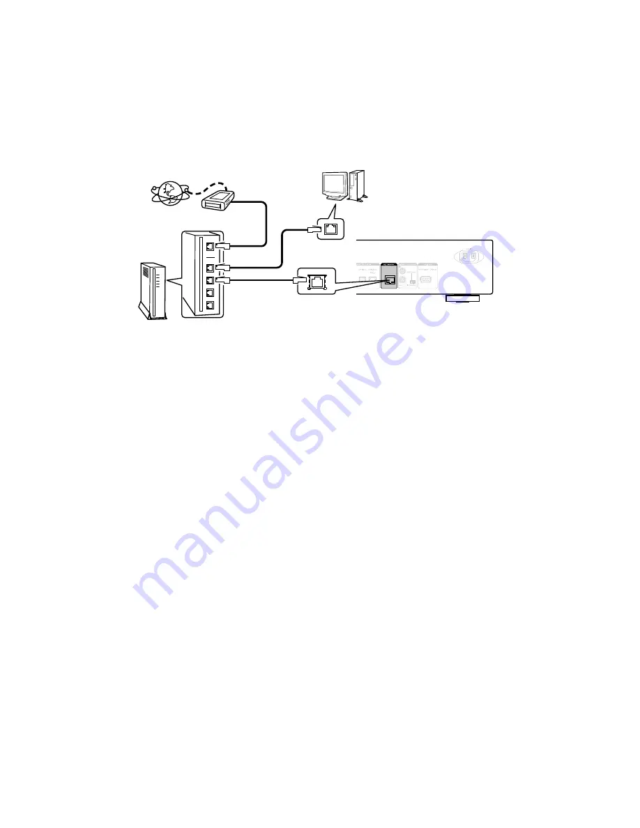
2.1.  Network Connection

(1)  System Requirements
• 

A broadband internet connection

• Modem
• Router
• 

Ethernet cable (CAT-5 or greater recommended)

(2) Settings

2.2.  Check and update the firmware

Check whether new firmware is available. It is also possible to check approximately how long the update will take.

(1)  Turn on the power pressing ON/STANDBY button.

(2)   Press INPUT and Cursor 

u

i

 buttons. Select the Setup, then press ENTER button.


 Press Cursor 

u

i

 buttons select to General. Press ENTER button. 


 Press Cursor 

u

i

 buttons select to Firmware. Press ENTER button. 


 Press Cursor 

u

i

 buttons select to Update. Press ENTER button. 


 Press Cursor 

u

i

 buttons select to Check for Update. Press ENTER button.

(3)   Press the ENTER button.

 The latest version of the firmware uploaded to the web is displayed.


 If the latest firmware version is on the web, proceed to (4).


 If the latest firmware is already installed, press the INPUT button to close the Update menu.

(4)  Press ENTER button. Select "YES", then press ENTER button.

(5)  Firmware Update will be started.

--- Precautions for Updates ---

•  The environment and settings must allow connection to broadband Internet for updates.
• Never turn off the power before an update is completed.
•  It takes around 1 hour to complete the update.
Once an update is started, normal operations cannot be performed until it is completed.

The GUI menu settings and image adjustment settings of this unit may be initialized.
Take note of your settings beforehand and reconfigure them after the update.

Modem

Internet

Computer

Computer LAN port / Ethernet connector

ETHERNET connector

Router

To WAN port

To LAN port

To LAN port

Summary of Contents for NA8005

Page 1: ...ome illustrations using in this service manual are slightly different from the actual set Please use this service manual with referring to the operating instructions without fail For purposes of improvement specifications and design are subject to change without notice Service Manual ...

Page 2: ...ess Rewrite Mode 18 9 Access to Development Server Mode 18 10 USB Update Mode by USB 18 11 Control 4 Identify Mode 18 Procedure after Replacing the Microprocessor etc 28 2 Updating by DPMS 29 Firmware Update Procedure 30 1 Updating by USB 30 TROUBLE SHOOTING 28 1 Power not turn on 28 2 OLED doesn t Light 30 3 No Sound Noise generated 32 MEASURING METHOD AND WAVEFORMS 39 BLOCK DIAGRAM 41 POWER DIAG...

Page 3: ...vice manual What you can do with this manual Search for a Ref No phrase Ctrl Shift F You can use the search function in Acrobat Reader to search for a Ref No in schematic diagrams block diagrams and parts lists 1 Press Ctrl Shift F on the keyboard The Search window appears 2 Enter the Ref No you want to search for in the Search window and then click the Search button A list of search results appea...

Page 4: ...g Adobe Reader 9 On the Document menu click Sign Magnify schematic printed wiring board diagrams 1 Ctrl Space mouse operation Press Ctrl Space on the keyboard and drag the mouse to select the area you want to view The selected area is magnified When you want to move the area shown hold down Space and drag the mouse When you want to show a full page view press Ctrl 0 on the keyboard Ctrl Space 0 Pr...

Page 5: ...een Example using Adobe Reader 9 On the Tools menu point to Select Zoom and then click Pan Zoom Window Magnify schematic printed wiring board diagrams 3 Loupe Tool function The Loupe Tool function lets you magnify a specific part of a diagram in a separate window Example using Adobe Reader X On the View menu point to Zoom and then click Loupe Tool The Loupe Tool window appears on the screen Exampl...

Page 6: ...tant safety parts that are indicated by the z mark on schematic diagrams and parts lists be sure to use the designated parts Be sure to mount parts and arrange the wires as they were originally placed For safety seasons some parts use tapes tubes or other insulating materials and some parts are mounted away from the surface of printed circuit boards Care is also taken with the positions of the wir...

Page 7: ...problem is identified and remedied NOTICE ALL RESISTANCE VALUES IN OHM k 1 000 OHM M 1 000 000 OHM ALL CAPACITANCE VALUES ARE EXPRESSED IN MICRO FARAD UNLESS OTHERWISE INDICATED P INDICATES MICRO MICRO FARAD EACH VOLTAGE AND CURRENT ARE MEASURED AT NO SIGNAL INPUT CONDITION CIRCUIT AND PARTS ARE SUBJECT TO CHANGE WITHOUT PRIOR NOTICE INSTRUCTIONS FOR HANDLING SEMI CONDUCTORS AND OPTICAL UNIT Elect...

Page 8: ...Personal notes 8 ...

Page 9: ...lanced output 2 3 V RMS PCM 1 7 V RMS DSD Headphone output 30 mW 32 Ω ohms variable maximum Digital output Coaxial 0 5 Vp p 75 Ω ohms Optical 15 21 dBm Digital input Coaxial 0 5 Vp p 75 Ω ohms Optical 27 dBm or lator USB Front USB Type A USB 2 0 High speed USB Rear USB Type B USB 2 0 High speed n n General Power supply voltage frequency F AC 100V 50 60Hz Power supply voltage frequency N AC 230 V 5...

Page 10: ...itialization Factory Initialization Factory Reset Press the INPUT and CURSOR DOWN f buttons simultaneously while inserting the AC plug to turn the power on Factory Reset appears on the display See SPECIAL MODE on page 11 for details on the differences between the different types of initialization 3 The unit then changes to the normal mode NOTE If the status in step 3 does not occur start again fro...

Page 11: ...taken from the top of the unit The photograph is NA8005U1B model The viewpoint of each photograph Shooting direction X View from the top Shooting direction B Shooting direction C Shooting direction A Shooting direction D Front side FRONT PANEL ASSY See DISASSEMBLY 1 FRONT PANEL ASSY and EXPLODED VIEW FRONT PCB Ref No of EXPLODED VIEW P1 STANDBY PCB Ref No of EXPLODED VIEW P3 PHONE PCB Ref No of EX...

Page 12: ...ing CABINET TOP FRONT PANEL ASSY 1 Remove the screws 3 Remove the connector wires and FFC Remove the screws CN81 FFC Cable CN19 カッ ト See EXPLODED VIEW for instructions on how to remove each PCB of the FRONT PANEL ASSY Bottom side ...

Page 13: ...8 2 DIGITAL PCB Proceeding CABINET TOP DIGITAL PCB 1 Remove the screws 2 Remove the screws Remove the connector wires and FFC DIGITAL PCB CN15 FFC Cable CN14 FFC Cable カッ ト ...

Page 14: ...ew 2 Remove the screws Remove the connector wires and FFC 4 POWER PCB Proceeding CABINET TOP POWER PCB 1 Remove the screws Remove the connector wires and FFC SMPS PCB CN91 CN92 CN93 カッ ト POWER PCB CN19 CN85 CN95 カッ ト WF91 BN14 BN93 CN96 カッ ト Shooting direction A ...

Page 15: ...10 5 AUDIO PCB Proceeding CABINET TOP AUDIO PCB 1 Remove the screws 2 Remove the connector wires and remove the screws AUDIO PCB FFC cable CN81 CN98 Shooting direction A ...

Page 16: ... detailes 2 Updating by DPMS on page 29 3 Version display d CURSOR UP Version Display 4 Product mode 2 INPUT 0 CURSOR LEFT Factory use 5 Protection History Display INPUT d CURSOR UP Latest view of Protection history 6 DPMS force update mode 8 FAST REWIND d CURSOR LEFT DPMS update 7 Update by RS232C 8 FAST REWIND f CURSOR UP Development Factory use 8 MAC Address rewrite 8 FAST REWIND 1 CURSOR RIGHT...

Page 17: ...ewriting failed log Clear the history of protection Startup display All lights on display And light the STANDBY LED Orange DISPLAY OFF LED Red DIGI OUT OFF LED Red 2 seconds All lights on display And light the STANBY LED Orange 2 seconds Factory Reset displayed for 5 seconds Initialization Items Default setting Default INPUT Internet Radio DIMMER 100 Favorite list Clear all iPod mode Direct mode A...

Page 18: ...d Startup display Initialized is displayed for 5 seconds 3 Version Display Mode Menu items appear in the Add Version Otherwise normal operation To exit this mode unplug the power cord Startup display Version is displayed for 5 seconds How to Display Version Press INPUT buttom and Cursor u Cursor i to select the Setup Then press ENTER button Press ENTER button System u com version is displayed Pres...

Page 19: ...14 Press Cursor i buttom Image version for the network microprocessor is displayed Press Cursor i buttom USB DAC version is displayed Press Cursor i buttom Sireal number is displayed Serial MZ_bccdddddd ...

Page 20: ... state Network No Connection or Unsupported Disc or continue no operation and Stop state Digital In No Input unlock To exit this mode unplug the power cord 5 Protection History Display Mode Startup display Product Mode2 is displayed for 5 seconds To exit this mode unplug the power cord No history found DC protection occurred Case B B was short circuit 12V_D 12V_A 12V_A or 29V was failed How to del...

Page 21: ...lure TimeOut Turn off and on the power Updating starts automatically 11 Firm Info response acquisition recived error Main rewrite Firmware recived failure Error Turn off and on the power Updating starts automatically 12 Firm Info response acquisition recived error Main rewirte Firmware recived data incorrect CheckSumError Turn off and on the power Updating starts automatically 13 Rewrite failure B...

Page 22: ...off and on the power Updating starts automatically Carry out the update in an environment that has little network load A7 FirmInfo Get Response TimeOut Turn off and on the power Updating starts automatically Carry out the update in an environment that has little network load A8 Net not connected Check the network connection Carry out the update in an environment that has little network load A9 Net...

Page 23: ...it this mode unplug the power cord 10 USB Update Mode by USB Turn on the AC plug while pressing the button of FAST REWIND 8 and CURSOR LEFT 0 at the same time See detailes 1 Updating by USB on page 30 11 Control 4 Identify Mode Hold down buttons STOP 2 and CURSOR DOWN f for at least 3 seconds while the power is on The Identify function for a Control4 compat ble device is executed The following is ...

Page 24: ...19 Personal notes ...

Page 25: ...t A The software has been written The software is not written at the time of replacement B The software has been written The software may need to be rewritten by version updates Check the version C The software has not been written The software needs to be written after replacement See Firmware Update Procedure for information on writing the software D The software has been written Be sure to rewr...

Page 26: ...or Update Press ENTER button 3 Press the ENTER button The latest version of the firmware uploaded to the web is displayed If the latest firmware version is on the web proceed to 4 If the latest firmware is already installed press the INPUT button to close the Update menu 4 Press ENTER button Select YES then press ENTER button 5 Firmware Update will be started Precautions for Updates The environmen...

Page 27: ...nnected to the USB connector on the front of the unit Turn on the AC plug while pressing the button of FAST REWIND 8 and CURSOR LEFT 0 at the same time The following message appears on the display Press the ENTER button and firmware update starts on this unit if updating all devices hold down buttons INPUT for at least 3 seconds The following message appears on the display This unit is turned off ...

Page 28: ... Is the control signal 3 3V SMPS PCB CN93 3pin STB_CNT Is the control signal 3 3V DIGITAL PCB IC11 pin98 A_power_on off Check Soldering or replace DIGITAL PCB IC11 Is D964 anode 0V SMPS PCB Next page Is the Fuse opened SMPS PCB F951 Replace F951 Insert wire properly Is D960 Cathode around 6V SMPS PCB Replace TF91 or IC95 Is IC92 6pin 3 9V SMPS PCB YES NO NO NO NO NO NO NO YES YES YES YES YES NO YE...

Page 29: ... 1 2NET 3 3V WF91 9pin CTL 3 3NET 3 3V WF91 11pin CTL 3 3DSP 3 3V WF91 13pin CTL 1 8DSP 3 3V Check DC voltage POWER PCB IC903 4pin 3 3V IC901 4pin 1 2V IC907 2pin 3 3V IC908 3pin 1 8V IC909 3pin 1 2V IC912 2pin 3 3V IC904 3pin 5V Check control signal DIGITAL PCB IC11 77pin NET 3 3 STB 3 3V IC11 99pin CTL 5USBA 3 3V IC11 61pin CTL 1 2NET 3 3V IC11 63pin CTL 3 3NET 3 3V IC11 119pin CTL 3 3DSP 3 3V I...

Page 30: ...ck Wire BN85 Check device POWER PCB IC910 2pin 3 3V Is DC voltage normal POWER PCB CN85 6pin 3 3V Check Wire BN85 Check Wire BN85 Replace IC81 NO NO NO NO NO YES YES YES YES YES YES NO YES YES Check device POWER PCB IC907 2pin 3 3V Check device POWER PCB Fuse F902 Check reset signal DIGITAL Board U6002 25pin EL RESET 3 3V Check Soldering or replace DIGITAL PCB IC11 Check Soldering or replace DIGIT...

Page 31: ...L RESET 26pin EL E RD 27pin EL DC 28pin EL R W _WR 29pin EL_CS Check Soldering or replace DIGITAL PCB IC11 NO YES END Check FFC cable Check Soldering WF81 1pin 27pin WF11 1pin 27pin Check Soldering FRONT PCB WF81 13 20pin DA0 DA7 25pin EL RESET 24pin EL RD 23pin EL DC 22pin EL RW 21pin EL CS ...

Page 32: ...in the playback mode AUDIO PCB D763 Cathode 14V Is the Fuse opened AUDIO PCB F601 F602 F603 Replace each Fuse Insert the wire properly Check Soldering or replace each device Check the control signal in playback mode AUDIO PCB WF61 19pin playback mode 3 3V Check Soldering or replace DIGITAL PCB IC11 or AUDIO PCB IC70 YES NO NO NO YES YES YES YES NO NO Check soldering or replace Q631 D763 D764 ...

Page 33: ...42 26pin DIR_CE Chip enable IC42 34pin DIR_RST Reset 3 3V Is I2S signal normal DIGITAL PCB IC44 12pin LRCK_DSDR 32KHz 192KHz IC44 9pin BCK_DSDCLK 2 112MHz 12 288 MHz IC44 4pin SDA DSDL IC44 48pin 512Fs 16 38MHz 24 576MHz Check DC voltage DIGITAL PCB L402 3 3V Check Soldering DIGITAL PCB CN14 5pin 3 3DD Check Soldering or replace DIGITAL PCB JK54 JK55 R513 R516 C529 etc Check Soldering or replace D...

Page 34: ... each clock normal in playback mode DIGITAL PCB WF12 5pin 512Fs WF12 7pin SDA_DSDL WF12 9pin BCK_DSDCLK WF12 11in LRCK_DSDR Go to 3 3 DAC Check Soldering or replace DIGITAL PCB WF12 R181 R182 R183 NO YES YES ...

Page 35: ...3V Check Soldering or replace AUDIO PCB IC61 Is DAC input signal normal in playback mode AUDIO PCB IC61 3pin SDA DSDL DATA INPUT IC61 4pin BCK DSDCLK 2 112MHz 12 288MHz IC61 5pin LRCK DSDR 32kHz 192kHz IC61 6pin MCLK 22 579MHz or 24 576MHz Check Soldering or replace AUDIO PCB IC61 IC64 IC65 IC66 IC67 R691 694 R638 R640 R663 etc Check Soldering or replace AUDIO PCB IC61 IC70 WF61 R688 R669 YES YES ...

Page 36: ... 3pin NET3 3V 3 3V CN15 2pin NET1 2V 1 2V Go to 1 power not turn on NO NO NO Check DC voltage DIGITAL PCB CN14 9PIN 5V Is SPDIF output normal DIGITAL PCB R477 BCO SPDIF Pulse Replace DIGITAL PCB Go to 1 power not turn on Go to 3 2 COAXAL OPTICAL YES NO YES ...

Page 37: ...eck I2S signal DIGITAL PCB IC42 29pin USBB_LRCK LRCK clock 32KHz 192KHz IC42 30pin USBB_BCK BCK clock 2 112MHz 12 288 MHz IC42 28pin USBB_DATA PCM data Go to 3 2 COAXIAL OPTICAL Check Master clock DIGITAL PCB IC42 31pin USBB_MCK 22 5792MHz or 24 576MHz Check Soldering or replace AUDIO PCB IC63 X601 X602 IC65 WF61 R637 R678 Check soldering or replace R437 R475 RN34 or DIGITAL PCB NO NO NO YES YES Y...

Page 38: ...38 Personal notes ...

Page 39: ...oints CUP12586Z AUDIO PCB TEST POINT CUP12585Z DIGITAL PCB TEST POINT q MCLK R694 w SCLK R692 e LRCK R693 r SDIN R691 t BCK_DSDCLK R182 y LRCK_DSDR R183 u SDA_DSDL R181 i DIR_BCK R434 o DIR LRCK R435 Q0 DIR_DATA R436 Q1 DAC_BCK R420 Q2 DAC_LRCK R418 Q3 DAC_DATA R419 r q w e r t y u i Q0 o Q2 Q1 Q3 39 ...

Page 40: ... FS 48K IC61 CS4398 pin6 MCLK IC61 CS4398 pin6 MCLK IC61 S4398 pin4 SCLK R692 IC61 S4398 pin5 LRCK R693 IC61 S4398 pin3 SDIN R691 IC61 S4398 pin4 SCLK R692 IC61 S4398 pin5 LRCK R693 IC61 S4398 pin3 SDIN R691 IC44 LCX157 pin9 BCK_DSDCLK R182 IC44 LCX157 pin12 LRCK_DSDR R183 IC44 LCX157 pin 4 SDA_DSDL R181 IC44 LCX157 pin9 BCK_DSDCLK R182 IC44 LCX157 pin12 LRCK_DSDR R183 IC44 LCX157 pin 4 SDA_DSDL R...

Page 41: ...S SW Digital Out Buffer 22 5792 MHz SW USB DAC DSP TM320C6748 GND HDAM LPF AMP Isolator SYSTEM uCOM USB Type B USB Type A Clock 30 00 MHz Standby Control 24 576 MHz V RC 5 IN OUT RC 5 INT EXT Front IR sensor System uCOM RS232C Flasher R232C System uCOM RS232 Audio 1 V Audio 1 V Audio 14V Audio 14V Isolator Isolator MCK BCK_DSDCLK LRCK_DSDR SDA_DSDL V CLK Serial Flash GD25Q32B SMPS only standby mod...

Page 42: ...1 D915 IC903 D910 D954 D956 D961 IC95 TF91 6SMPS IC93 D916 IC92 D911 3 9SMPS BCO RS232C D919 IC910 u CON 18V OLED 3 3DSP 3 3NET RELAY 5V 5USBA ANALOG TRANS 1 8DSP 1 2V 1 2DSP STANDBY SMPS 1 2NET 1 8V BCO 3 3DD FET SW 3 3V 15V 15V for Audio 5V 5DIGO 5V V 5D1 for Audio 15V 15V for Audio 3 9V V 3 3D1 for Audio 3 3V 3 3ST 3 3V 1 8SMPS 1 8V DC DC Converter 3 9V DC DC Converter POWER DIAGRAM 42 ...

Page 43: ...WIRING DIAGRAM 43 ...

Page 44: ... B SIDE Lead free Solder When soldering use the Lead free Solder Sn Ag Cu PRINTED CIRCUIT BOARDS 1 2 3 4 5 6 7 8 9 10 11 12 13 14 15 16 A B C D E F G H J K L M A B C D E F G H J K L M 1 2 3 4 5 6 7 8 9 10 11 12 13 14 15 16 ...

Page 45: ...45 POWER A SIDE SMPS A SIDE POWER B SIDE SMPS B SIDE 1 2 3 4 5 6 7 8 9 10 11 12 13 14 15 16 A B C D E F G H J K L M A B C D E F G H J K L M 1 2 3 4 5 6 7 8 9 10 11 12 13 14 15 16 ...

Page 46: ...IGITAL B SIDE FRONT A SIDE FRONT B SIDE STANDBY A SIDE PHONE A SIDE STANDBY B SIDE PHONE B SIDE 1 2 3 4 5 6 7 8 9 10 11 12 13 14 15 16 A B C D E F G H J K L M A B C D E F G H J K L M 1 2 3 4 5 6 7 8 9 10 11 12 13 14 15 16 ...

Page 47: ... Q601 2SK2145GR 3 G2 S D2 G1 D1 2 4 5 1 Q701 2SK2145GR Q654 Q653 C686 0 1u C687 0 01u C751 3300u 25V AO C752 3300u 25V AO 8 7 6 5 4 3 2 1 IC65 ADuM1286CRZ D602 1SS355T D603 1SS355T D604 1SS355T D605 1SS355T D606 1SS355T D607 1SS355T D608 1SS355T 8 7 6 5 4 3 2 1 IC66 ADuM1285CRZ 8 7 6 5 4 3 2 1 IC67 ADuM1285CRZ 8 7 6 5 4 3 2 1 IC68 ADuM1280ARZ 8 7 6 5 4 3 2 1 IC69 ADuM1280ARZ 8 7 6 5 4 3 2 1 IC70 A...

Page 48: ...4 2 2K R159 OPEN R160 OPEN R161 OPEN R158 10K R150 10K R101 0 R102 0 C116 100 16V C115 47 16V C113 47 16V C106 47 16V C117 0 1uF C114 0 1uF C110 0 1uF R103 10K R104 10K R105 10K C104 0 1uF C105 0 1uF R106 10K R107 22 R108 22 R109 0 R110 0 R111 0 R112 OPEN R113 0 R114 0 R115 0 1 2 3 4 5 6 7 8 IC12 R1EX24256BSAS0A R177 4 7K R178 4 7K C111 0 1uF R116 0 R117 0 R118 0 R119 0 R120 0 R121 0 R122 0 R123 0...

Page 49: ...DD14 T6 LCDD10 T7 LCDD6 T8 LCDD2 T9 LCD_CTRL1 T10 LCDCLK T11 MIIITXER T12 MIIRXCLK T13 MIICOL T14 MII RXDV T15 FD5 T16 FD6 T17 FD7 T18 D15 U1 AV2_DATA0 U2 AV3_CTRL0 U3 AV4_DATA1 U4 LCDD16 U5 LCDD13 U6 LCDD9 U7 LCDD5 U8 LCDD1 U9 LCD_CTRL2 U10 MIITXD0 U11 MIITXD2 U12 MIIRXD0 U13 MIIRXD2 U14 MIIMDIO U15 NFCE0 U16 FCLE U17 NFWE U18 NFRB V1 NC 06 V2 AV4_DATA0 V3 LCDD17 V4 LCDD15 V5 LCDD12 V6 LCDD8 V7 L...

Page 50: ... 06 V17 VP DIN 03 V18 VP DIN 15 V19 VP DIN 14 W1 OUT IN00 W2 OUT IN01 W3 OUT IN02 W4 DDR A 10 W5 DDR A 06 W6 DDR A 02 W7 DDR CLK N W8 DDR CLK P W9 DDR RASN W10 DDR D 15 W11 DDR D 07 W12 DDR D 06 W13 DDR DQM 0 W14 INT USBB W15 IN OUT10 W16 VP DIN 04 W17 VP DIN 02 W18 VP DIN 01 W19 VP DIN 00 IC31 CVITMS320C6748BZWT C430 0 1uF C439 4700P C438 0 068uF R481 680 C440 100 16V C437 0 1uF R480 470 R479 OPE...

Page 51: ...0 1 R519 0 R521 OPEN R522 0 R529 47 R530 0 C553 OPEN R528 OPEN R525 33 R526 22 C552 100P C551 47 16V R532 51 R533 51 R534 51 R535 51 Q505 HVTKRA102S Q504 HVTKRC102S 1 2 3 4 5 6 SW51 KSS2B016Z D505 CVD1SS355T Q501 OPEN C510 0 1uF C512 1000P C514 0 1uF C513 220P D503 OPEN D504 OPEN C509 220P C511 1000P D515 KDS160 D506 CVD1SS355T Q503 HVTKRA102S D508 CVD1SS355T D507 OPEN R507 0 R508 47 C521 0 1uF C5...

Page 52: ...0 1uF 11 10 9 8 7 6 5 4 3 2 1 BN14 CWB11 L903 BLM21AG121 L904 BLM21AG121 L906 BLM21AG121 L907 BLM21AG121 L908 BLM21AG121 21 20 19 18 17 16 15 14 13 12 11 10 9 8 7 6 5 4 3 2 1 WF91 CJP21GA115ZY R928 0 R929 0 R930 0 R931 0 R932 0 R933 0 R934 0 R935 0 R936 0 R937 33 R938 33 L909 BLM21AG121 L910 BLM21AG121 L911 BLM21AG121 R939 OPEN R940 0 R941 10K 3 VOUT VCC GND C CTL 2 4 5 1 IC903 CVIBA00JC5WTHA 3 VO...

Page 53: ...2 OPEN R979 OPEN Q951 KTD1863ATP R956 OPEN 1 2 3 4 IC97 PC17L1CB LF91 CLZ9Z086Z 8 7 6 5 4 3 2 1 IC95 CVIICE3B0365J CX92 0 1 250V CX93 470P AC250V CX91 0 1 250V BK19 CJT1A026 CY94 0 01uF AC250V CY95 0 01uF AC250V R984 33 R983 33 CY96 2200P 250V R982 220 1 2 3 4 5 6 7 8 9 10 11 CN93 CJP11GI236ZW C957 10 50V C956 0 1uF D953 1N4003 R965 100K C978 22uF 25V 8 7 6 5 4 3 2 1 IC92 DB1230HE C992 10V 2 2uF R...

Page 54: ...804 PAUSE S805 PLAY R841 180 R842 270 R843 390 S806 UP R844 150 S807 DOWN S808 RIGHT S809 LEFT S810 ENTER R845 180 R846 270 R847 390 C802 0 1uF C809 0 1uF R848 1K R849 1K C810 0 1uF C811 0 1uF C812 0 1uF 5 3 1 2 CON VIN GND VADJ VOUT 4 IC81 CVINJM2387ADL3 C813 50V 22uF C814 0 1uF R850 15K R851 8 2K R852 1K R853 1K C815 47 25V C816 0 1uF L805 BLM21PG22 D808 2 7V R854 0 R855 0 R856 1M R857 0 R858 0 ...

Page 55: ...x5 S4 S4 S9 x4 S4 x4 S5 x4 S8 x2 S8 x4 S8 x1 S3 x1 S1 x1 S7 x2 S5 x2 S6 x3 S6 x3 S4 x1 S4 x1 S4 x2 S4 x7 S2 x5 S3 x2 M11 M12 M12 M12 P10 S4 x1 S6 x1 S10 x4 M13 M14 M14 S4 x1 S4 x1 x2 x2 S4 x4 S11 x1 S11 x1 S11 x1 Please see the last chapter for the part list EXPLODED VIEW WARNING Parts marked with this symbol z have critical characteristics Use ONLY replacement parts recommended by the manufacture...

Page 56: ...Personal notes Personal notes 56 ...

Page 57: ...8 8 3 3 3 3 1 1 2 2 7 9 5 6 10 11 4 4 4 4 4 2 3 2 8 8 1 2 14 13 1 5 6 15 UK plug UK Only PACKING VIEW Please see the last chapter for the part list z 57 ...

Page 58: ...TORS Only major semiconductors are shown general semiconductors etc are omitted to list The semiconductor which described a detailed drawing in a schematic diagram are omitted to list 1 IC s R5F56108VNFP MAIN IC 11 ...

Page 59: ...29 EL CS O EL CS L Communication enable with OLED L O L O L 30 D7 O Data Bus for OLED L O L O L 31 D6 O Data Bus for OLED L O L O L 32 D5 O Data Bus for OLED L O L O L 33 D4 O Data Bus for OLED L O L O L 34 D3 O Data Bus for OLED L O L O L 35 D2 O Data Bus for OLED L O L O L 36 D1 O Data Bus for OLED L O L O L 37 D0 O Data Bus for OLED L O L O L 38 SCK USBB O USBB E VOL I2C CLOCK OUTPUT L O L O L ...

Page 60: ...C Control L O L O L 80 DAC_MDO O OPEN L O L O L 81 DAC MC O DAC Control L O L O L 82 REMOTE OUT O Remote Output signal L O H O H PU 83 DSD PCM_OUT O DSD or PCM Switching signal L O L O L 84 OPEN O OPEN L O L O L 85 DIR USB O DIR USBB Switching L O L O L 86 DIR_DO I DIR Control L I I 87 DIR DI O DIR Control L O L O L 88 DIR CL O DIR Control L O L O L 89 DIR_CE O DIR Control L O L O L 90 DIR_RERR I ...

Page 61: ... LED_DISP_OFF O LED Control DISPLAY OFF L O L O L PD 126 LED DIGOUT OFF O LED Control DIGITAL OUT OFF L O L O L PD 127 TEST4 I Port for Setting up PWB CHECK MODE L I I PD 128 LED_NOR_STB O LED Control NORMAL STANDBY L O L O L PD 129 LED_NET_LED O LED Control NETWORK STANDBY H O L O H PD 130 VSS GND L 131 OPEN O OPEN L O L O L PD 132 VCC 3 3V CPU H 133 REGION I Region ID PORT 0V E2 0 43V JP 0 82V E...

Page 62: ...62 PCM9211 DIGITAL IC42 PCM9211 Block Diagram ...

Page 63: ...63 PCM9211 Pin Discriptions ...

Page 64: ...3 TDI TDI PLD UPDATE IN Test Data Input for JTAG 24 TCK TCK PLD UPDATE IN Test Clock for JTAG 25 TDO TDO PLD UPDATE OUT Test Data Out for JTAG 26 IO SLAVE_MCK CD MECHA OUT CD MECHA MCK 33 8688MHz 27 IO DAC_DSD_DATAL DSD1792A OUT DAC_DSD_DATAL 28 IO DAC_DSD_DATAR DSD1792A OUT DAC_DSD_DATAR 29 IO DAC DSD BCK DSD1792A OUT DAC DSD BCK 30 IO DAC_LRCK DSD1792A OUT DAC_LRCK 31 VCCIO1 33_VCCIO DA3 3V Powe...

Page 65: ...S320C6748BZWT3 IN USBB_DSD_DATA_L 69 IO USBB_DSD_DATA_ R TMS320C6748BZWT3 IN USBB_DSD_DATA_R 70 IO CD USBB DIR M3062LFGPGP IN MODE CD USBB DIR Detect 71 IO NC CS2000 NC 72 IO USBB_MUTE TMS320C6748BZWT3 IN USBB Mute Control 73 IO NC NC 74 IO NC NC 75 IO NC NC 76 IO INT EXT M3062LFGPGP IN INT EXT selection port 77 IO D_MUTE M3062LFGPGP IN Moni USBB_PCM DSD MUTE timing 78 IO DAC_CONT_SEL M3062LFGPGP ...

Page 66: ...66 CS2000 CP DIGITAL IC43 CS2000 CP Block Diagram ...

Page 67: ... BMUTEC AMUTEC 18 25 Mute Control Output The Mute Control pin is active during power up initialization mut ing power down or if the master clock to left right clock frequency ratio is incorrect During reset these outputs are set to a high impedance AOUTB AOUTB 20 19 Differential Right Channel Analog Output Output The full scale differential analog output level is specified in the Analog Characteri...

Page 68: ...A VIB GND1 VDD2 VIA VOB GND2 10444 005 Figure 5 ADuM1281 ADuM1286 Pin Configuration Table 21 ADuM1281 ADuM1286 Pin Function Descriptions Pin No Mnemonic Description 1 VDD1 2 7 V to 5 5 V Supply Voltage for Isolator Side 1 2 VOA Logic Output A 3 VIB Logic Input B 4 GND1 Ground 1 Ground reference for Isolator Side 1 5 GND2 Ground 2 Ground reference for Isolator Side 2 6 VOB Logic Output B 7 VIA Logi...

Page 69: ...69 MFI337S3959 DIGITAL IC25 ...

Page 70: ...70 2 DISPLAY S020 MXS4035A 3 ...

Page 71: ...09 231810071508S IC REGULATOR HVIPQ012ENB1ZPH 1 IC910 90M HC300740R REGULATOR 3 3V OUTPUT LOWDROP KIA278R33PI HVIKIA278R33PI 1 IC912 943229500020S MOSFET TPC6111 P CH U MOSV TPC6111 TOSHIBA CVTTPC6111 1 IC92 93 943239100820D I C DC DC CONVERTER 3A 700KHZ SOP 8P CVIDB1230HETR 2 IC94 90M HC300770R I C REGULATOR KIA431B HVIKIA431BAT 1 IC95 943235003220S IC CooLSET ICE3B0365J ICE3B0365J DIP 8P NF NEON...

Page 72: ...A22605020 CAP ELECT 25V 22uF 22UF 25V CCEA1EH220T 1 C962 nsp CAP CERAMIC 1kV 2200pF K EKR3A222K05FK5 CCKT3A222KBL 1 C978 981 nsp CAP CHIP 2012 25V 22uF X7R SAMSUNG CL21B226KAFNNNE CCUC1E226KCS 4 C982 nsp CAP CHIP 1608 50V 1500pF X7R SAMSUNG CL10B152KB8NNNC CCUS1H152KCS 1 C983 nsp CAP CH P 1608 50V 1000pF X7R _SAMSUNG CL10B102KB8NNNC CCUS1H102KCS 1 C984 985 nsp CAP CH P 1608 50V 0 01uF X7R _SAMSUNG...

Page 73: ...POWER 3 REF No Part No Part Name Remarks Q ty New Ver nsp HEAT SINK CMY4A222 V2 1 nsp SCREW CTB3 8JR 1 nsp HEAT SINK CMY4A222 V2 1 nsp SCREW CTB3 8JR 1 ...

Page 74: ...4 nsp RES CHIP 1608 5 47Kohm CRJ10DJ473T 1 RC81 262010007707S SENSOR REMOTE 367KHz HM336R GOOD TAKE CRVHM336R 1 CAPACIITORS GROUP C801 nsp CAP CHIP 1608 50V 100pF C0G SAMSUNG CL10C101JB8NNNC CCUS1H101JAS 1 C802 803 nsp CAP CHIP 1608 50V 01uF X7R SAMSUNG CL10B104KB8NNNC CCUS1H104KCS 2 C804 nsp CAP ELECT 16V 47uF S CCEA1CKS470T 1 C805 806 nsp CAP CHIP 1608 50V 1000pF X7R _SAMSUNG CL10B102KB8NNNC CCU...

Page 75: ...RITE CH P BEAD 2012 220R BLM21PG221SN1 MURATAMURATA CLZBLM21PG221SN1 1 PH81 90M YT004500R JACK PHONES 635mm SILVER PJ 612A 51 YUQIU CJJ2E026Z 1 S801 812 00D9430004402 SW TACT SKHV10910G CST1A012ZT 12 VR81 00D9430196908 RES VARIABLE CVV2J02B103Z 1 WF81 nsp WAFER FFC 125mm ANGLE 125 2S NPW CJP27GB286ZN 1 WF82 nsp WAFER FPC FFC 30P 1mm PITCH ANGLE FPC 10S 12X NPW CJP30GB305ZN 1 963179100040S OLED MOD...

Page 76: ...SK880 TOSHIBA CVT2SK880GR 2 Q653 nsp HEATSINK ASS Y CVT2SD2081 CMY2A223 V2 CVT2SD2081 CMY2A223 V2 CVT2SD2081JA 1 Q654 nsp HEATSINK ASS Y CVT2SB1259 CMY2A223 V2 CVT2SB1259 CMY2A223 V2 CVT2SB1259JA 1 Q655 00MHX300012AY T R 2SC4116 NPN SC 70 TOSHIBA 2SC4116 TOSHIBA CVT2SC4116 1 Q656 212050002507S T R 2SA1586 PNP SC 70 TOSH BA 2SA1586 TOSH BA CVT2SA1586 1 Q701 943222500200D F E T 2SK2145 N CH 2 3L1C L...

Page 77: ...PROPYLENE FAS 133 200VDC 470KTP FAS 133 200VDC470KTPSH NYEI CCMP2B470KS17T 1 C609 610 00MOA227016Z0 CAP ELECT 16V 220uF ELNA ROS ELNA ROS 16V 220UF CCEA1CR221T 2 C614 615 00MOA227025R0 CAP ELECT 220UF 25V 10X20 ELNA ROA CCEA1EROA221T 2 C616 nsp CAP CH P 1608 50V 0 01uF X7R _SAMSUNG CL10B103KB8NNNC CCUS1H103KCS 1 C617 nsp CAP CH P 1608 50V 0 1uF X7R _SAMSUNG CL10B104KB8NNNC CCUS1H104KCS 1 C618 nsp ...

Page 78: ...SUNG CL10B103KB8NNNC CCUS1H103KCS 1 C789 nsp CAP CH P 1608 50V 0 1uF X7R SAMSUNG CL10B104KB8NNNC CCUS1H104KCS 1 C790 nsp CAP CH P 1608 50V 1000pF X7R SAMSUNG CL10B102KB8NNNC CCUS1H102KCS 1 C791 nsp CAP CH P 1608 50V 0 1uF X7R SAMSUNG CL10B104KB8NNNC CCUS1H104KCS 1 C792 nsp CAP CH P 1608 50V 0 01uF X7R SAMSUNG CL10B103KB8NNNC CCUS1H103KCS 1 C793 nsp CAP CH P 1608 50V 1000pF X7R SAMSUNG CL10B102KB8N...

Page 79: ...00D2690192902 TR CH P SOT 23 KRC102S HVTKRC102S 1 Q301 302 00D2690192902 TR CH P SOT 23 KRC102S HVTKRC102S 2 Q303 943229500020S MOSFET TPC6111 P CH U MOSV TPC6111 TOSHIBA CVTTPC6111 1 Q503 00D2690184907 TR CH P SOT 23 KRA102S HVTKRA102S 1 Q504 00D2690192902 TR CH P SOT 23 KRC102S HVTKRC102S 1 Q505 00D2690184907 TR CH P SOT 23 KRA102S HVTKRA102S 1 Q506 507 00D2690192902 TR CH P SOT 23 KRC102S HVTKR...

Page 80: ... CRJ10DJ220T 3 R476 nsp RES CH P 1608 5 10Kohm CRJ10DJ103T 1 R477 nsp RES CH P 1608 5 0ohm CRJ10DJ0R0T 1 R478 nsp RES CH P 1608 5 22ohm CRJ10DJ220T 1 R480 nsp RES CH P 1608 5 470ohm CRJ10DJ471T 1 R481 nsp RES CHIP 1608 5 680ohm CRJ10DJ681T 1 R482 484 nsp RES CHIP 1608 5 22ohm CRJ10DJ220T 3 R485 nsp RES CHIP 1608 5 0ohm CRJ10DJ0R0T 1 R486 nsp RES CHIP 1608 5 10Kohm CRJ10DJ103T 1 R487 497 nsp RES CH...

Page 81: ...P CH P 1005 16V 01uF X7R _SAMSUNG CL05B104KO5NNNC CCUI1C104KCS 9 C343 nsp CAP CH P 1608 16V 022uF X7R _SAMSUNG CL10B224KO8NNNC CCUS1C224KCS 1 C344 367 nsp CAP CH P 1005 16V 01uF X7R _SAMSUNG CL05B104KO5NNNC CCUI1C104KCS 24 C368 nsp CAP CH P 1005 25V 001uF X7R _SAMSUNG CL05B103KA5NNNC CCUI1E103KCS 1 C369 nsp CAP CHIP 1005 16V 01uF X7R SAMSUNG CL05B104KO5NNNC CCUI1C104KCS 1 C370 nsp CAP CHIP 1005 25...

Page 82: ...50V 1000pF X7R SAMSUNG CL10B102KB8NNNC CCUS1H102KCS 1 C585 586 nsp CAP CH P 1608 50V 100pF C0G SAMSUNG CL10C101JB8NNNC CCUS1H101JAS 2 C587 nsp CAP CH P 1005 50V 1000pF X7R SAMSUNG CL05B102KB5NNNC CCUI1H102KCS 1 C589 nsp CAP CH P 1005 25V 001uF X7R _SAMSUNG CL05B103KA5NNNC CCUI1E103KCS 1 C590 nsp CAP CH P 1005 16V 01uF X7R _SAMSUNG CL05B104KO5NNNC CCUI1C104KCS 1 C591 nsp CAP CH P 1005 50V 470pF C0G...

Page 83: ...2A175UA 1 F13 943412101320M ENTER KNOB ASS Y SG CGK1A176UA 1 F13 943412101330M ENTER KNOB ASS Y B CGK1A176TA 1 F14 943411103250M BUTTON INPUT SG CBT1A1190RMD10 1 F14 943411103250M BUTTON INPUT B CBT1A1190 1 F15 943411103270M CURSOR BUTTON ASS Y SG CGK2A175TA 1 F15 943411103280M CURSOR BUTTON ASS Y B CGK2A175SA 1 F16 943411103290M PLAY BUTTON ASS Y SG CGK1A176SA 1 F16 943411103300M PLAY BUTTON ASS ...

Page 84: ... 4 3 54111112202AM MANUAL GETT NGSTART F CQX1A1776Z 1 4 3 54111112200AM MANUAL GETT NGSTART U CQX1A1775Z 1 4 3 54111112201AM MANUAL GETT NGSTART N CQX1A1774Z 1 4 3 54111112203AM MANUAL GETT NGSTART K CQX1A1777Z 1 4 4 nsp CARD USER JAPAN F CQE1A139S 1 4 5 nsp SHEET ADDRESS JAPAN F CQE1A195N 1 4 5 nsp CARDFORCHINAINDENTIFICATION K CQE1A450Z 1 4 6 nsp CARD WARRANTY U CQE1A131V 1 4 6 nsp WARRANTYCANAD...

Reviews: