Implementing MLC NAND Flash for Cost-Effective, High-Capacity Memory
91-SR-014-02-8L
4
e
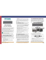
-
Oxide
Floating
Gate
Select Gate
Source
Drain
Substrate
Program
(Inject electrons)
Erase
(Remove electrons)
Figure 1: A Basic Flash Cell
Binary and MLC Technologies
In flash devices that implement Binary flash technology, there are two possible ranges for V
Th
. MLC
technology can have several valid ranges for V
Th
, instead of just two. The first implementation of
MLC uses four voltage levels (see Figure 2). Each state is mapped to one of four combinations of
two bits. Therefore, the cell can store two bits of data.
Figure 2 also shows some of the complexity caused by the migration from Binary flash to MLC. The
programming and erase processes become more complicated since the circuits must maintain tighter
V
Th
tolerances. This translates into longer program and erase times, and a more complicated read
process.
Figure 2: Voltage Level Comparison between Binary and Flash Technologies