15
dc2151af
DEMO MANUAL DC2151A
Information furnished by Linear Technology Corporation is believed to be accurate and reliable.
However, no responsibility is assumed for its use. Linear Technology Corporation makes no representa-
tion that the interconnection of its circuits as described herein will not infringe on existing patent rights.
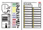
schematic Diagram
5
5
4
4
3
3
2
2
1
1
D
D
C
C
B
B
A
A
OVERVOLTAGE TOLERANT BUFFERS
TRANSLATE THE HIGH PULL-UP
VOLTAGES FROM THE LTC3330 TO THE
VOUT VOLTAGE DRIVING THE
PROCESSOR I/O BUS, WHICH IS VOUT.
U2, U3, U4 FUNCTION TABLE
II
I
Y
LL
L
HH
LL
L
02
21
0
Y= ( I ) ( I ) + ( I ) ( I )
.
.
75.0
56.2
R11
I_CHRG
5mA
113
BATTERY CHARGE
CURRENT *
10mA
7.5mA
*
12
VOUT
VOUT
EH_ON
PGVOUT
VOUT
VOUT
PGVOUT
EH_ON
VIN
BB_IN
FAST_CHRG
SIZE
DATE:
IC NO.
REV.
SHEET
OF
TITLE:
APPROVALS
PCB DES.
APP ENG.
TECHNOLOGY
Fax: (408)434-0507
Milpitas, CA 95035 Phone: (408)432-1900
1630 McCarthy Blvd.
LTC Confidential-For Customer Use Only
CUSTOMER NOTICE
LINEAR TECHNOLOGY HAS MADE A BEST EFFORT TO DESIGN A
CIRCUIT THAT MEETS CUSTOMER-SUPPLIED SPECIFICATIONS;
HOWEVER, IT REMAINS THE CUSTOMER'S RESPONSIBILITY TO
VERIFY PROPER AND RELIABLE OPERATION IN THE ACTUAL
APPLICATION. COMPONENT SUBSTITUTION AND PRINTED
CIRCUIT BOARD LAYOUT MAY SIGNIFICANTLY AFFECT CIRCUIT
PERFORMANCE OR RELIABILITY. CONTACT LINEAR
TECHNOLOGY APPLICATIONS ENGINEERING FOR ASSISTANCE.
THIS CIRCUIT IS PROPRIETARY TO LINEAR TECHNOLOGY AND
SCHEMATIC
SUPPLIED FOR USE WITH LINEAR TECHNOLOGY PARTS.
SCALE = NONE
www.linear.com
2
DEMO CIRCUIT 2151A
22
NANOPOWER BUCK - BOOST DC / DC
N/A
LTC3331EUH
NC
JD
2 - 21 - 14
WITH ENERGY HARVESTING BATTERY CHARGER
R11
56.2
R11
56.2
NDC7001C
Q1A
NDC7001C
Q1A
1
5
6
R12
1.00Meg
R12
1.00Meg
U3
NC7SZ58P6X
U3
NC7SZ58P6X
I1
1
GND
2
I0
3
Y
4
VCC
5
I2
6
R13
100k
R13
100k
J1
DUST HEADER 2X6
SMH-106-02-L-D-05
J1
DUST HEADER 2X6
SMH-106-02-L-D-05
VSUPPLY
1
NC
2
GND
3
PGOOD
4
KEY
5
VBAT
6
RSVD
7
EHORBAT
8
I/O 2
9
I/O 1
10
+5V
11
V+
12
Q2
CMPT3906E
Q2
CMPT3906E
1
3
2
U2
NC7SZ58P6X
U2
NC7SZ58P6X
I1
1
GND
2
I0
3
Y
4
VCC
5
I2
6
R14
1.00Meg
R14
1.00Meg
D1
CMOSH-3
D1
CMOSH-3
2
1
Q1B
NDC7001C
Q1B
NDC7001C
3
2
4
Figure 19. DC2151A Demo Circuit Schematic, Page 2