


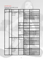

20
JT50/52
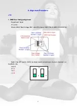
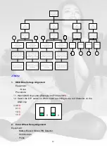
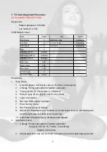
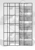
1. DMD Bias Voltage Alignment
Equipment:
-None
Procedure:
11. Watch DMD chip Label (Example: 9477000 0234
B
)
12. Switch the DIP switch on DMD board according to the red character on the
DMD chip
3. 00:
B
01:
C
10:
D
11:
E
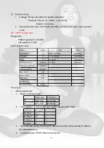
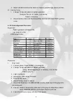
2. Color Wheel Delay Alignment
Equipment:
-
Battery Biased Silicon PIN Detector
-
Oscilloscope
-
Probe
0
0
Summary of Contents for RD-JT51
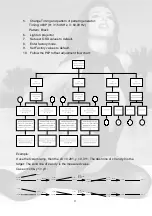
Page 13: ...13 2 JT50 52 ...
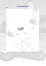
Page 14: ...14 7 Packaging Description 1 JT51 ...
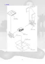
Page 15: ...15 2 JT50 52 ...
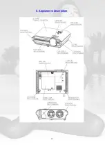
Page 16: ...16 8 Appearance Description ...
Page 53: ...ëí 5 PFC BOARD 6 DC DC BOARD ...
Page 54: ...ëì JT50 52 1 Final Assembly Trouble Shooting Guide ...
Page 55: ...ëë ...
Page 56: ...ëê 2 Engine Assembly Trouble Shooting Guide ...
Page 58: ...ëè 4 Power Supply Trouble Shooting Guide PFC BOARD DX850 DC DC BOARD ...
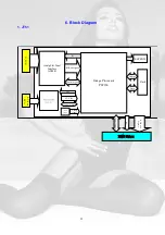
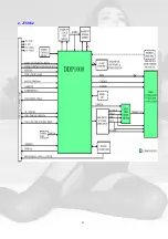
Page 59: ...5ç 5 DMD Block Trouble Shooting Guide ...
Page 60: ...êð ...
Page 74: ...éì Step 7 Download finished Step 8 Turn off the power switch ...
Page 81: ......


