52
135
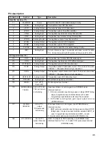
PDIAG#
Passed Diagnostics. This signal is asserted by Device 1 to
indicate to Device 0 that it has completed diagnostics.
132,137,134
HA2,HA1,HA0
Device Address Bus. This is the 3-bit binary coded address
provided by the host to access an ATA register or data.
131
CS1FX#
Host Chip Select1 (for 1Fxh/17xh). This is the chip select signal
from the host to select the Command Block Registers.
130
CS3FX#
Host Chip Select2 (for 3Fxh/37xh). This is the chip select signal
from the host to select the Command Block Registers.
129
DASP#
Device Active/Device 1 Present. This is a time-multiplexed signal
that indicates that a device is active, or that Device 1 is present.
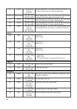
GIO (3)
168
GIOO
General IO0.
Default : input.
169
GIO1
General IO1.
Default : input.
170
GIO2
General IO2.
Default : input.
196
GIO3/PHTIN
1. General IO3.
Default : input.
2. For receiving high track count signal PHTO from 1616.
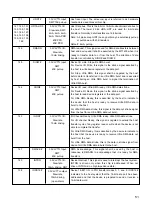
TEST (2)
173
PRST
Power on reset input, high active.
172
TEST
Test mode, active high
RF SIO (5)
191
ASPREQ
ASP request signa input from MT1616 to get RECD1, XTOR,
DEFECT automatically.
175
XRST#
RF reset output. Active low.
190
XDATA
Data signal output for RF register setting.
187
XLAT#
Latch signal output for RF register setting.
188
XCLK
Carrier clock signal output for RF register setting.
3.3V LVTTL I/O,
Slew rate,
10mA driving,
SMT, 40K pull-up
3.3V LVTTL Input,
SMT, 40K pull-up
3.3V LVTTL Input,
SMT, 40K pull-up
3.3V LVTTL Input,
SMT, 40K pull-up
3.3V LVTTL I/O,
Slew rate,
10mA driving,
SMT, 40K pull-up
3.3V LVTTL output,
SMT,
4mA driving,
75K pull-down
3.3V LVTTL output,
SMT,
4mA driving,
75K pull-down
3.3V LVTTL output,
SMT,
4mA driving,
75K pull-down
3.3V LVTTL output,
SMT,
4mA driving,
75K pull-down
3.3V LVTTL input,
SMT,
3.3V LVTTL input,
75K pull-down
3.3V LVTTL input,
SMT,
75K pull-down
3.3V LVTTL output,
4mA driving
3.3V LVTTL I/O,
Slew rate,
75K pulll-down,
4mA driving
3.3V LVTTL output,
4mA driving
3.3V LVTTL output,
Slew rate,
8mA driving


