3. TECHNICAL BRIEF
- 13 -
Copyright © 011 LG Electronics. Inc. All right reserved.
Only for training and service purposes
LGE Internal Use Only
3. TECHNICAL BRIEF
3.1.2 DDR1 Memory (MT46V16M16P-6TIT, U201)
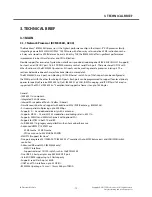
The MT46V16M16P-6TIT is a 256Mb Double Data Rate(DDR) SDRAM. The DDR SDRAM uses a double data rate
architecture to achieve high-speed operation. The double data rate architecture is essentially a 2
n-prefetch
architecture with an interface
designed to transfer two data words per clock cycle at the I/O pins. A single read or
write access for the DDR SDRAM effectively consists of a single 2
n-bit-wide, one-clockcycle
data transfer at the internal DRAM core and two corresponding
n-bit-wide, onehalf-
clock-cycle data transfers at
the I/O pins.
VDD = +2 5V
·
0 2V VDDQ = +2 5V
·
0 2V
• VDD = +2.5V
·
0.2V, VDDQ = +2.5V
·
0.2V
• VDD = +2.6V
·
0.1V, VDDQ = +2.6V
·
0.1V (DDR400)
• Bidirectional data strobe (DQS) transmitted/received with data, that is, source-synchronous data capture
(x16 has two – one per byte)
• Internal, pipelined double-data-rate (DDR) architecture; two data accesses per clock cycle
• Differential clock inputs (CK and CK#)
• Commands entered on each positive CK edge
• DQS edge-aligned with data for READs; centeraligned with data for WRITEs
DLL t
li
DQ
d DQS t
iti
ith CK
• DLL to align DQ and DQS transitions with CK
• Four internal banks for concurrent operation
• Data mask (DM) for masking write data (x16 has two – one per byte)
• Programmable burst lengths (BL): 2, 4, or 8
• Auto refresh
– 64ms, 8192-cycle(Commercial & Industrial)
– 16ms, 8192-cycle (Automotive)
• Self refresh (not available on AT devices)
L
l d TSOP f i
d li bili (OCPL)
• Longer-lead TSOP for improved reliability (OCPL)
• 2.5V I/O (SSTL_2-compatible)
• Concurrent auto precharge option supported
• 66-pin TSOP (Pb-free) (22.22mm x 11.76mm x 1.2mm)
CKE
CK#
CK
DQ0-DQ15
LDQS
256Mb
DDR1 SDRAM
Memory
CK
CS#
WE#
CAS#
RAS#
A0-A12
BA0,BA1
LDQS
UDQS
LDM
UDM
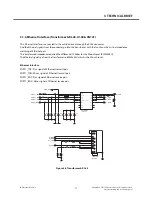
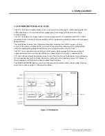
Figure 3.2 MT46V16M16P-6TIT Block Diagram
BA0,BA1


