27
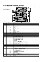
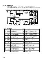
IC201 (H8/3062) : µ-COM
It Controls the total system giving or taking the data from the peripheral ICS.
•
Pin Description
Pin
No.
1
2
3
4
5
6
7
8
9
10
11
12
13
14
15
16
17
18
19
20
21
22
23
24
25
26
27
28
29
30
31
32
33
34
35
36
37
38
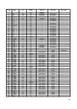
DRD-8080B
pin name
VCC1
RCLK
LDON
XCS
DSPMUTE
SLGNCHG
LINK
XRST
LED
FWE
VSS1
SIDATA
TRAYOUT/TXD
XILAT
SQCK/RXD
SICLK
SCLK
LAYERVD-0
LAYERVD-1
SPDG0
SPDG1
VSS2
SHORTBRK
AUDMUTE
RFCTL
FWEON
D0
D1
D2
D3
D4
D5
D6
D7
VCC2
A0
A1
A2
5V
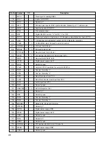
SP3723 control clock
APC output On/Off to SP3723
Chip select to CXD1867
Mute signal to CXD3030R
Sled drive Gain Change
LINK signal monitor output to SP3723
Reset out to CXD3030R, 1867R
Access LED
Flash memory writing enable input from Q201 emitter
GND
Serial Data signal to CXD3030R
Tray open output to BA5983
Serial data latch output
Sub Q serial clock to CXD3030R
Serial clock signal to CXD3030R
SENS serial clock to CXD3030R
Offset input for Focus actuator to Q503 base
Offset input for Focus actuator to Q504 base
Spindle Gain control signal 0
Spindle Gain control signal 1
GND
Short brake output signal to spindle driver IC 401
Audio Mute Control
RF signal Pass change
Flash memory writing enable output to Q201 base
Data bus to CXD1867R
Data bus to CXD1867R
Data bus to CXD1867R
Data bus to CXD1867R
Data bus to CXD1867R
Data bus to CXD1867R
Data bus to CXD1867R
Data bus to CXD1867R
5V
Address bus to CXD1867R
Address bus to CXD1867R
Address bus to CXD1867R
H8/3062
pin name
Vcc
PB-0
PB-1
PB-2
PB-3
PB-4
PB-5
PB-6
PB-7
FWE
Vss
P9-0
P9-1
P9-2
P9-3
P9-4
P9-5
P4-0
P4-1
P4-2
P4-3
Vss
P4-4
P4-5
P4-6
P4-7
D8
D9
D10
D11
D12
D13
D14
D15
Vcc
P1-0
P1-1
P1-2
I/O
I
O
O
I
O
O
O
O
O
I
I
O
O
O
O
O
O
O
O
O
O
I
O
O
O
O
I/O
I/O
I/O
I/O
I/O
I/O
I/O
I/O
I
O
O
O
Description


