41
Notes :
• The data at the 32-bit slot is output in 2's complements on an LSB-first basis. The data at the 48-bit slot is
output in 2's complements on an MSB-first basis.
• GTOP monitors the state of Frame Sync protection. ("H" : Sync protection window released)
• XUGF is a negative Frame Sync pulse obtained from the EFM signal before Frame Sync protection is
effected.
• XPLCK is an inversion of the EFM PLL clock. The PLL is designed so that the falling edge of XPLCK
coincides with a change point of the EFM signal.
• The GFS signal turns "H" upon coincidence between Frame Sync and the timing of interpolation protection.
• RFCK is a signal generated at 136-µs periods using a crystal oscillator.
• C2PO is a signal to indicate data error.
• XRAOF is a signal issued when a jitter margin of
+
28F is exceeded by the 32K RAM.
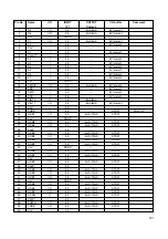
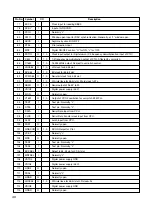
Pin No.
Symbol
I/O
Description
116
PCMD48 O
1, 0
D/A interface for 48-bit slot serial data
117
HDBC
O
Normally open
118
BCK48
O
1, 0
D/A interface for 48-bit slot bit clock
119
VDIO3
Digital power supply (3.8V)
120
HDBB
O
Normally open
121
GTOP
O
1, 0
GTOP output
122
HDBA
O
Normally open
123
XUGF
O
1, 0
XUGF output
124
VSIO4
Digital power supply GND
125
HDB9
O
Normally open.
126
C2PO
O
1, 0
C2PO output
127
HDB8
O
Normally open
128
XRAOF
O
1, 0
XRAOF output
129
VDC3
Digital power supply (2.5V)
130
XTL2
O
Normally open
131
XTL1
I
Normally “L”
132
VSC3
Digital GND
133
AVS3
Analog GND
134
PWM2N
O
1, 0
PWM output for Audio DAC. Rch, Reverse phase
135
PWM2P
O
1, 0
PWM output for Audio DAC. Rch, Forward phase
136
AVD3
Analog power supply (2.5V)
137
AVD4
Power supply for master clock
138
XTLO
O
1, 0
X’tal oscillation circuit output of master clock.
139
XTL1
I
X’tal oscillation circuit input of master clock.
140
AVS4
GND for master clock
141
AVS5
Analog GND
142
PWM1P
O
1, 0
PWM output for Audio DAC. Lch, Forward phase
143
PWM1N
O
1, 0
PWM output for Audio DAC. Lch, Reverse phase.
144
AVD5
Analog power supply (2.5V)


