background image


Page: 30 


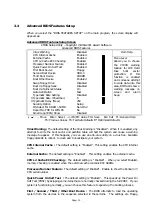
3.4      Advanced BIOS Features Setup   


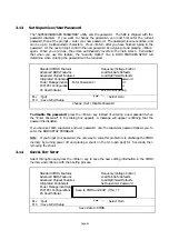
When you select the “BIOS FEATURES SETUP” on the main program, the screen display will 

appears as: 


Advanced BIOS Features Setup Screen 

CMOS Setup Utility – Copyright © 1984-2001 Award Software 

Advanced BIOS Features 

Item Help 


    X 


Virus Warning 

CPU Internal Cache 

External Cache 

CPU L2 Cache ECC Checking 
Processor Number Feature 

Quick Power On Self Test 

First Boot Device 

Second Boot Device 

Third Boot Device 

Boot Other Device 
Swap Floppy Drive 

Boot Up Floppy Seek 

Boot Up NumLock Status 

Gate A20 Option 

Typematic Rate Setting 

Typematic Rate (Chars/Sec) 

Typematic Delay (Msec) 
Security Option 

OS Select For DRAM >64MB 

Report No FDD for WIN 95 

Small Logo (EPA) Show 

Disabled 

Enabled 

Enabled 

Enabled 
Enabled 

Enabled 

Floppy   

HDD-0 

CDROM 

Enabled 
Disabled 

Disabled 

On 

Fast 

Disabled 

250 
Setup 

Non-OS2 

No 

Disabled 

Menu Level   
Allows you to choose 

the VIRUS warning 

feature for IDE Hard 

Disk boot sector 

protection. If this 

function is enabled 

and someone attempt 
to write data into this 

area, BIOS will show a 

warning message on 

screen and alarm 

beep. 

á


â


àß

 Move   Enter: Select  +/-/PU/PD: Value  F10: Save    Esc: Exit  F1: General Help   

F5: Previous Values  F6: Fail-Safe Defaults F7: Optimized Defaults 


Virus Warning : 

The default setting of the Virus Warning is “Disabled”.  When it is enabled, any 

attempt to write the boot sector and partition table will halt the system and cause a warning 

message to appear.  If this happens, you can use an anti-virus utility on a virus free, bootable 

floppy diskette to reboot, to clean and to investigate your system. 


CPU Internal Cache : 

The default setting is “Enabled”. This setting enables the CPU internal 

cache. 


External Cache : 

The default setting is “Enabled”.  This setting enables the external cache. 


CPU L2 Cache ECC Checking : 

The default setting is “Enabled”.  When you select Enabled, 

memory checking is enabled when the external cache contains ECC SRAMs.


Processor Number Feature : 

The default setting is “Enabled”.  Enable to show the Pentium !!! 

CPU serial number.


Quick Power On Self Test  : 

The default setting is “Enabled”.  This speeds up the Power On 

Self Test (POST) by skipping some items that are normally checked during the full POST.  If your 
system is functioning normally, you can choose this feature to speed up the booting process. 


First / Second / Third / Other Boot Device : 

The BIOS attempts to load the operating 

system from the devices in the sequence selected in these items.  The settings are Floppy, 


Summary of Contents for EM-561 Series

Page 1: ...EM 561 SERIES 5 25 EMBEDDED SBC WITH VGA THREE 10 100MBPS LAN FOR SOCKET370 PENTIUM III PROCESSOR USER S MANUAL...

Page 2: ...of the manufacturer except for copies retained by the purchaser for backup purposes All rights are reserved TRADEMARKS The following are trademarks or registered trademarks of their respective compan...

Page 3: ...Setup 28 3 4 BIOS Features Setup 30 3 5 Chipset Features Setup 32 3 6 Integrated Peripherals 34 3 7 Power Management Setup 36 3 8 PnP PCI Configuration 39 3 9 PC Health Status 40 3 10 Frequency Voltag...

Page 4: ......

Page 5: ...ion connector with one PCI riser card one FDD interface support up to two floppy devices two IDE ports that support up to four IDE devices and Ultra ATA 100 66 33 interface helps designers and integra...

Page 6: ...llel port SPP EPP ECP Bus Interface PCI bus slot RTC Internal RTC with Li battery Keyboard Mouse 6 pin keyboard mouse pin header Watchdog Timer 16 level time out intervals Universal Serial Bus Support...

Page 7: ...Page 3 1 5 Board Layout...

Page 8: ...d open it by first pulling the lever of socket upward Step 2 Insert the CPU into the socket Please keep the lever right angle when inserting CPU Step 3 When inserting the CPU please note the correct o...

Page 9: ...downward to hock the ear of socket firmly Step 7 Finally attach the fan cable to the CPU fan header 2 1 2 System Memory Installation Step 1 Open latches of DIMM socket Step 2 Insert the RAM module in...

Page 10: ...same direction 2 2 JUMPER SETTINGS AND CONNECTORS 2 2 1 Board Outline CON2 PWR1 IDE1 IDE2 FDC1 Cyrix COM1 JP5 MS LAN1 LAN2 LAN3 CON1 JP3 JP2 JP1 JP12 JP15 ATXC1 JP13 JP14 JP6 SDOC1 PCI1 KM1 JP8 DIMI J...

Page 11: ...JP15 Factory use only l JP8 Clear CMOS Data Description JP8 Normal Default 1 2 Clear CMOS 2 3 l JP11 Select CPU Clock CPU Clock Speed JP11 66MHz 3 5 4 6 100MHz 1 3 4 6 100 133MHz Default 1 3 2 4 JP8 3...

Page 12: ...Page 8 l JP6 Flash FWH Chip Flash FWH chip JP6 Unlocked Default 1 2 Locked 2 3 l JP7 Case Open Detect Case Open Detect JP7 Enable Default ON Disable OFF JP7 JP6 1 2 3 JP6 JP7...

Page 13: ...mming 3 4 DOC1 Select DiskOnChip Flash Disk Address Flash Disk Address Sdoc1 CC00 CDFFH 1 2 9 10 D000 D1FFH 3 4 7 8 D400 D5FFH 3 4 9 10 D800 D9FFH 5 6 7 8 DC00 DDFFH 5 6 9 10 Default SDOC1 1 3 5 7 9 2...

Page 14: ...X Power Header JP1 JP2 JP3 Extension LAN LED FAN1 CPU FAN Connector COM1 RS 232 Serial Port 1 Connector COM2 Serial Port 2 Connector CON1 Power LED Reset Speaker Connector USB1 2 3 4 USB Port 1 2 3 4...

Page 15: ...Page 11 LAN1 LAN2 LAN3 LAN Connector Pin No Description 1 TX 2 TX 3 RX 4 NC 5 NC 6 RX 7 NC 8 NC 1 8 LAN1 LAN2 LAN3 LAN1 LAN2 LAN3...

Page 16: ...4 Auto Form Feed 2 Data0 15 Error 3 Data1 16 Initialize 4 Data2 17 Printer Select IN 5 Data3 18 Ground 6 Data4 19 Ground 7 Data5 20 Ground 8 Data6 21 Ground 9 Data7 22 Ground 10 Acknowledge 23 Ground...

Page 17: ...e Connector Pin No Description 1 Keyboard Data 2 Mouse Data 3 Ground 4 5V 5 Keyboard Clock 6 Mouse Clock 7 NC 8 NC lPWR1 HDD Power Connector Pin No Description 1 5V 2 Ground 3 Ground 4 12V 1 2 3 4 PWR...

Page 18: ...Page 14 ATXB1 ATX Power On Off Header Pin No Description 1 PANSW 2 GND ATXC1 ATX Power Header Pin No Description 1 GND 2 Standby 5V 3 GND 4 PSON ATXC1 1 4 ATXB1 1 2 ATXPB1 ATXC1...

Page 19: ...AN LED Pin No Description 1 10 100M LED 2 10 100M LED 3 LINK LED 4 LINK LED 5 Active LED 6 Active LED FAN1 CPU FAN Connector Pin No Description 1 Ground 2 12V 3 FAN Status Signal JP1 JP2 JP3 1 3 5 2 4...

Page 20: ...6 Data Set Ready DSRA 7 Request To Send RTSA 8 Clear To Send CTSA 9 Ring Indicator RIA lCOM2 Serial Port 2 Connector Header Pin No Description 1 Data Carrier Detect DCDB 2 Receive Data RXDB 3 Transmi...

Page 21: ...LED Reset Speaker Connector Pin No Description 1 Power LED 2 GND 3 HDD LED 4 HDD LED 5 RESET SW 6 RESET SW GND 7 External Speaker 8 Internal Buzzer 9 NC 10 External Speaker Default 7 8 ON Internal Bu...

Page 22: ...B D0 3 USB D0 4 Ground USB1 5 USB Port 1 Vcc 1 USB Port 2 Vcc 2 USB D1 3 USB D1 4 Ground USB2 5 USB Port 2 Vcc 1 USB Port 3 Vcc 2 USB D2 3 USB D2 4 Ground USB3 5 USB Port 3 Vcc 1 USB Port 4 Vcc 2 USB...

Page 23: ...8 Index 9 Ground 10 Motor Enable A 11 Ground 12 Drive Select B 13 Ground 14 Drive Select A 15 Ground 16 Motor Enable B 17 Ground 18 Direction 19 Ground 20 Step 21 Ground 22 Write Data 23 Ground 24 Wr...

Page 24: ...VGA1 VGA Connector Pin No Description Pin No Description 1 Red Signal 2 Ground 3 Green Signal 4 Ground 5 Blue Signal 6 Ground 7 H SYNC 8 Ground 9 V SYNC 10 Ground 11 DDC DATA 12 DDC Clock 1 2 11 12 VG...

Page 25: ...3 GND 13 GND 4 5V 14 Power On Switch 5 GND 15 GND 6 5V 16 GND 7 GND 17 GND 8 Power Good 18 5V 9 5V Stand By 19 5V 10 12V 20 5V lPS1 AT Power Connector For EM 561C only Pin No Description 1 Power Good...

Page 26: ...Data 10 9 Data 4 10 Data 11 11 Data 3 12 Data 12 13 Data 2 14 Data 13 15 Data 1 16 Data 14 17 Data 0 18 Data 15 19 Ground 20 NC 21 DMA REQ 22 Ground 23 IOW 24 Ground 25 IOR 26 Ground 27 IOCHRDY 28 NC...

Page 27: ...Data 10 9 Data 4 10 Data 11 11 Data 3 12 Data 12 13 Data 2 14 Data 13 15 Data 1 16 Data 14 17 Data 0 18 Data 15 19 Ground 20 NC 21 DMA REQ 22 Ground 23 IOW 24 Ground 25 IOR 26 Ground 27 IOCHRDY 28 NC...

Page 28: ...V B21 AD29 A22 AD28 B22 GND A23 AD26 B23 AD27 A24 GND B24 AD25 A25 AD24 B25 3 3V A26 IDSEL B26 C BE3 A27 3 3V B27 AD23 A28 AD22 B28 GND A29 AD20 B29 AD21 A30 GND B30 AD19 A31 AD18 B31 3 3V A32 AD16 B3...

Page 29: ...59 5V IO A60 REQ64 B60 ACK64 A61 5V B61 5V A62 5V B62 5V SR1 System Status Signal Port 440 Pin No Description 1 LED Signal 2 LED Signal EX For System Status Signal Port 440 bit 3 C DOS DEBUG O 440 8 S...

Page 30: ...diagnostic checks while initializing the board hardware If the routines encounter an error during the tests the error will be reported in either of the two different ways hear a series of short beeps...

Page 31: ...move cursor to your desired selection F1 General Help F5 Previous Values F6 Fail Safe Defaults F7 Optimized Defaults F10 Saves all changes made to Setup and exits program PU PD Change Value Standard...

Page 32: ...No Errors Base Memory 640K Extended Memory 260096K Total Memory 261120K Move Enter Select PU PD Value F10 Save Esc Exit F1 General Help F5 Previous Values F6 Fail Safe Defaults F7 Optimized Defaults...

Page 33: ...stations 2 Highlight the listing after each drive name and select the appropriate entry Video Select the type of primary video subsystem in your computer The BIOS usually detects the correct video typ...

Page 34: ...Save Esc Exit F1 General Help F5 Previous Values F6 Fail Safe DefaultsF7 Optimized Defaults Virus Warning The default setting of the Virus Warning is Disabled When it is enabled any attempt to write...

Page 35: ...choices range from 6 to 30 Chars Sec The default setting is 6 Chars Sec Typematic Delay M Sec This setting controls the time between the display of the first and second characters There are four dela...

Page 36: ...ber of clock cycles of CAS latency depends on the DRAM timing Do not reset this field from the default value specified by the system designer SDRAM Cycle Time Tras Trc This item allows you to select t...

Page 37: ...t delay transactions cycles Select Enable to support compliance with PCI specification version 2 1 AGP Graphic Aperture Size Select the size of the Accelerated Graphics Port AGP aperture The aperture...

Page 38: ...isabled PCI Slot Enabled BUTTON ONLY Enter Ctrl F1 Enabled 3F8 IRQ4 2F8 IRQ3 Normal Half 378 IRQ7 SPP 3 Off Move Enter Select PU PD Value F10 Save Esc Exit F1 General Help F5 Previous Values F6 Fail S...

Page 39: ...e KB power on function Hot Key Power On If POWER ON Function is set to Hot Key and then you can assign a hot key combination in the field for the PS 2 keyboard to power on the system Available options...

Page 40: ...y IDE 0 Disabled Secondary IDE 1 Disabled FDD COM LPT Port Disabled PCI PIRQ A D Disabled Move Enter Select PU PD Value F10 Save Esc Exit F1 General Help F5 Previous Values F6 Fail Safe DefaultsF7 Opt...

Page 41: ...rts and write blank to the video buffer Blank Screen This option only writes blanks to the video buffer DPMS Initial display power management signaling Suspend Mode Option are from 1 Min to 1 Hour and...

Page 42: ...e system boot up until it goes to the operating system before this function will work Reload Global Timer Events When Enabled an event occurring on each device listed below restarts the global time fo...

Page 43: ...initialize the PnP cards used for booting VGA IDE SCSI The rest of the cards will be initialized by the PnP operating system like Windows 95 or 98 When set to No BIOS will initialize all the PnP card...

Page 44: ...bled Item Help CPU_Voltage 1 58V Menu Level 3V STANDBY 3 26V 3 3V 3 21V 5V 4 83V 12V 11 64V 12V 12 11V 5V 5 15V 1 8V 1 61V CPU Temperature 38 Fan 1 Speed 4687 RPM Move Enter Select PU PD Value F10 Sav...

Page 45: ...Enabled and Disabled Spread Spectrum Modulated When the system clock generator pulses the extreme values of the pulse generate excess EMI Enabling pulse spectrum spread modulation changes the extreme...

Page 46: ...efault values for the most stable minimal performance system operations 3 12 LOAD OPTIMIZED DEFAULTS When you press Enter on this item you get a confirmation dialog box with a message similar to Stand...

Page 47: ...h Status Exit Without Saving Esc Quit Select Item F10 Save Exit Setup Change Set Disable Password To disable the password press the Enter key instead of entering a new password when the Enter Password...

Page 48: ...res Frequency Voltage Control Advanced BIOS Features Load Fail Safe Defaults Advanced Chipset Features Load Optimized Defaults Integrated Peripherals Set Supervisor Password Power Management Setup Set...

Page 49: ...install to the target system the Windows INF files that outline to the operating system how the chipset components will be configured This is needed for the proper functioning of the following feature...

Page 50: ...in9x The directory contains graphics drivers for Intel R 810 810E 815 815E Chipsets in Microsoft Windows 95 98 Millenium Please refer to readme txt first before running the auto installing program set...

Page 51: ...e 47 4 3 DRIVER SETUP INSTALLATION 4 3 1 Intel 815 chipset Driver Setup Setp 1 Run Driver CD ROM Setp 2 Directory EM 561 Series corechip Disk1 Setup exe Setp 3 Click Next 1 Click Here 2 Double Click H...

Page 52: ...Page 48 Setp 4 Setp 5 Setp6 Click Yes Click Next Click Finish...

Page 53: ...Page 49 4 3 2 Intel Ultra ATA Storage Driver Install Setp 1 Directory EM 561 Series corechip intelata063_multi exe Setp 2 Setp 3 1 Click Here 2 Double Click Here Click Next Click Yes...

Page 54: ...Page 50 Setp 4 Setp 5 Setp 6 Click Next Click Next Click Finish...

Page 55: ...Page 51 4 3 3 VGA Driver Install Step 1 Step 2 Setp 3 Double Click Display 1 Select Settings Click Advanced Click Change Select Adapter...

Page 56: ...Page 52 Step 4 Step 5 Step 6 Click Next Click Next Click Next 1 Put Driver CD ROM 2 Directory EM 561 Series Video xx...

Page 57: ...Page 53 Step 7 Step 8 4 3 4 LAN Driver Install Setp 1 Click Finish Click Next Double Click Control Panel...

Page 58: ...Page 54 Setp 2 Setp 3 Setp 4 Double Click System Double Click PCI Ethernet Control Click Update Driver...

Page 59: ...Page 55 Setp 5 Setp 6 Setp7 Click Next Click Next Click Next 1 Select Specify a location 2 Put Driver CD ROM 3 Find LAN Driver file...

Page 60: ...Page 56 Setp 8 Setp 9 Setp 10 Click Next 2 Click OK Click OK 1 Put win98 CD ROM...

Page 61: ...Page 57 Setp 11 Click Finish...

Page 62: ...rt 443H Step 2 Disable Output port 441H EX 1 For DOS Execute the DEBUG EXE file under DOS Then key in O443 The system will reboot automatically according to the time out you set Enable Disable C DOS D...

Page 63: ...turned at the customer expense 5 The following conditions are excluded from this warranty A Improper or inadequate maintenance by the customer B Unauthorized modification or misuse C Operation outside...

Page 64: ...press Others Item Model Name Serial Number Configuration Item Problem Code Failure Status Problem Code 01 D O A 02 Second Time R M A 03 CMOS Data Lost 04 FDC Fail 05 HDC Fail 06 Bad Slot 07 BIOS Probl...

Reviews: