background image


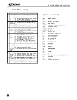
Chapter 6 Radio Debugging

Before test/debugging, make sure all the equipments have 

been well connected to the ground! 

Before test/debugging, make sure the antenna output terminal has 

been connected properly to the corresponding devices and load! 

The transmitter output must pass RF power attenuator before being 

c o n n e c t e d   t o   t h e   s t a n d a r d   s i g n a l   s o u r c e /   f r e q u e n c y  

deviator/frequency spectrum! 

When testing the receiver, make sure not to conduct transmitting 

operation! 

When in debugging/testing/service, make sure static free measures 

for human body and equipments.

6.1 Service Equipment and Software

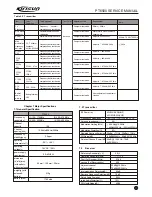
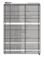
The following equipments and software in Table 6.1 are necessary 

for the service and test of the radio.

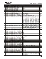
NO

  1

  2


  3


  4

  5


  6

  7

  8

  9

  10

  11

  12

  13

  14

Name

Computer

Programming 

software

Programming 

Cable

Cloning cable

DC regulated 

power

Therefore Power 

meter

Frequency meter

Frequency 

Deviator

Digital Multimeter

Audio Signal 

Generator

RF Power 

attenuator

Standard signal 

source

Oscillograph

Audio voltmeter


KSP6500

KSPL-09

KCL01

 5A

SWR

1.2

-6

1

10

0--

5kHz

Specifications

Above P2, compatible with IBM PC, 

WINDOWS 98/ME/2000/XP

Output voltage: 7.5V,  output current: 

Measuring rang: 0.5---10W
Frequency range: 100MHz500MHz

Impedance: 50Ù


Frequency range:  0.1600MHz
Frequency precision: higher than
Sensitivity: higher than 100mV

Frequency range: DC600MHz
Measuring range: 

Input impedance: higher than 10MÙ/V DC, 
w

ith the ability of testing voltage, current, 

impedance

Frequency range:  2---3000Hz
output level:  1---500mV

Attenuation: 40dB or 50dB
Supporting power: Bigger than 10W

Frequency range: 10MHz---1000MHz
Output level: 0.1uV~32mV (-127dBm~-
17dBm)
Frequency range:  DC~20MHz
Test range: 10mV~20V

Test range: 10mV~10V

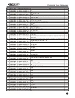
6.2 Debugging Items

During the course of maintenance, the radio needs to be 

tested and debugged after replacing components. Brief 

description of circuits is as follows.

Some certain radio parameters can be modified (computer 

mode) with our KSP6500 programming software. The 

modifiable parameters are as follows: 

1) Receiving and transmitting frequencies of different 

channels;

2) Receiving and transmitting signaling of different 

channels; 

3) Busy-lock selection of channels;

4) TOT transmitting time limit;

5) Squelch level;

6) Power-saving function selection;

7) 2-tone settings;

8) DTMF settings;

9) Voice alert function selection;

10) Monitoring mode selection;

11) Scanning mode selection;

12) Scanning reply channel selection;

13) Scanning channel priority selection;

14) Call list settings;

15) Customized alert;

Debugging Procedures: 

A, Enter the computer test mode. Access method refers to 

the instruction in 4.2.1 for entering the computer mode.

b, Select the Test Mode option in KPS6500 programming 

software to enter the computer test mode.

c, Select the options that you want to adjust and adjust the 

parameters on the computer.

d, After adjustment, exit the computer test mode.

6.3


Debugging

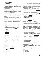
6.3.1 VCO Modification

Turn off the power saving mode. Set the frequency at the 

low frequency (see Table 6.2). In receiving status, test the PD 

power with the digital multimeter. Adjust the trimming capacitor 

C117 to make the PD power at 4.2V

0.1V

In the transmitting status, test the PD power with the digital 

multimeter and adjust the micro capacity C52 to make the 

voltage at PD point at 4.2V 0.1V

PT6500 SERVICE MANUAL

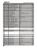
Recommendation: Equipment in item 6, 7, 8, 10, 11, and 12 
can be replaced by a comprehensive test instrument.

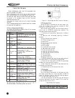
Figure 6.1   External Speaker/Mic. Connector Definition

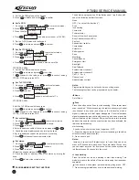
MIC JACK

MIC RXD

SPEAKER JACK

SP+

SP-

TXD

GND


400.125MHz

    435.125MHz

            469.975MHz

Table 6.2 Radio H/I/L Frequency

Low 

Frequency


Center 

frequency

Hi gh  Fr eq ue nc y        


14

Summary of Contents for PT6500

Page 1: ...PROFESSIONAL TWO WAY RADIO PT6500 V071208 FM PORTABLE RADIO SERVICE MANOAL Welcome ...

Page 2: ...ronic Shenzhen Co Ltd owns the trademarks KIRISUN PT6500 SERVICE MANUAL CONTENTS Chapter 1 Introduction 2 Chapter 2 Radio Overview and Function Keys 2 Chapter 3 Electrocircuit 3 Chapter 4 Function Description and Parameter Setting 7 Chapter 5 Service Assemble and Disassemble 12 Chapter 6 Radio Debugging 14 Chapter 7 Major Specifications 18 Chapter 8 Trouble Shooting 18 Appendix 1 Abbreviations 19 ...

Page 3: ...ight be used to apply for any components from Kirisun Component Application 1 3 Service All the Kirisun products are subject to the service warranty The main unit of the radio is guaranteed for free service of 24 months Accessories such as battery pack power adapter antenna or charger are guaranteed for free service of 6 months Earphones are wearing parts and out of warranty In one of the followin...

Page 4: ...limited at IC4 and then filtered at porcelain filter CF1 or CF2 450 kHz IC5 demodulates and sends out audio signals nd The 2 IF filter selector circuit consists of CF1 CF2 D18 D19 and peripheral circuits when the radio is set to broad band CF2 is open CF1 is closed and CF2 functions when the radio is set to narrow band CF1 is open CF2 is closed and CF1 functions Squelch Circuit Demodulation output...

Page 5: ...in21 DTMF 2T 5T signals etc DTMF 2T 5T signals etc come through the high pass circuit sub audio signals filtered consisting of Q30 and Q31 etc DTMF signals come to IC10 special chip for HT9172 DTMF decoding for decoding and then sent to MCU for processing 2T 5T signals are sent to MCU for processing after wave filtering and waveform modification by IC1 the other channel of signals voice signals ar...

Page 6: ...eiver and that of the transmitter are identical communication is available which avoids interference of other signals This radio is equipped with 39 groups of standard sub audio frequencies for your selection as shown in Table 1 CTCSS signals are generated by MCU PWM waveform and are sent to VCO for modulation via upper limiting filter consisting of RC which filters high frequency components over ...

Page 7: ...tter s VCO control switch VCO buffer amplifier Receiver s VCO control switch 3 4Semiconductor Function Description PT6500 SERVICE MANUAL Position IC10 IC11 IC14 IC2 IC3 IC4 IC5 IC6 IC7 IC8 IC9 Q1 Q10 Q11 Q12 Q12 Q13 Q14 Q15 Q16 Q17 Q18 Q19 Q2 Q20 Q21 Q22 Q23 Q24 Q25 Q26 Q29 Q3 Q30 Q31 Q32 Q33 Q34 Q35 Q36 Q37 Q38 Q39 Q4 Q40 Q41 Q42 Q43 Q44 Q45 Q47 Q48 Q49 Q5 Q51 Q6 Q7 Q8 Q9 41 42 43 44 45 46 47 48 ...

Page 8: ... programming Selected channel The channel selected by the scanning selector 4 1 4 1 2 0 7 PT6500 SERVICE MANUAL Specified Value 450kHz 6 0kHz or bigger 12 5kHz or smaller 2 0dB or smaller within f0 4kHz 6 0dB or smaller 47 0dB or bigger within f0 100kHz 1 5k Item Nominal center frequency 6dB bandwidth 50dB bandwidth Pulse Insertion loss Guarantee attenuation Terminal resistance Table 3 5 Diode Fun...

Page 9: ...lly added to the call list Enter the Call list menu by menu operation and select the sequence you want to call and press PTT for calling PT6500 SERVICE MANUAL knob Selected current channel The channel for holding call when receiving signals or the channel selected by the channel selection knob Priority 1 current channel The channel for Priority channel 1 or for holding call when receiving signals ...

Page 10: ... select mode 3 Press then Power Level is shown 4 Press to select e g Power Low 5 Change the power level with then press to confirm Set Companding 1 As shown in CH 1 press Utilities is shown 2 Press to enter select mode 3 Press and Companding is shown 4 Press to select Companding 5 Select On or OFF by press to confirm P4 P2 P3 P4 P4 P2 P3 P2 P3 P4 P4 P4 P4 P2 P3 P2 P3 P4 P4 P4 P4 P2 P3 P2 P3 P4 P4 ...

Page 11: ...s None OFF do not set the functions Scan lone working Contact list Power selector Show or hide the channel alias Busy Channel Lockout BCL Tx FRQ 401 660000 P3 P4 P1 Ch alias CHANNEL 1 P2 P3 P4 P4 Rx CTCSS 401 660000 P3 P4 P1 Ch alias CHANNEL 1 P2 P3 P4 P4 Tx CTCSS XXXX P3 P4 P1 P2 P3 P4 P4 P4 P2 P3 P2 P3 P4 P4 P4 P2 P3 Key lock Squelch level selector Companding Scrambler Battery power Zone Monitor...

Page 12: ...ntrast long press OFF 1 Press the key once Contrast will be shown 2 Press to select the character you need 3 Press to confirm Manual programming The dealer can open the manual programming rights of channel frequency set CTCSS DCS Basic operations of programmable keys You can set the programmable keys with the key set in PC software as follows It can be set as short press display channel frequency ...

Page 13: ...bulges of the battery pack with the corresponding at the rear of the transceiver To install the battery pack slots bottom Figure 5 1 1 Removing the Battery Pack To remove the battery pack use your thumb to press the belt clip one side of your index finger to press the release button and then pull the battery away from the radio 5 2 INSTALLING THE ANTENNA Screw the antenna into the connector at the...

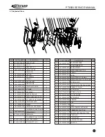
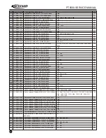
Page 14: ... ASSEBIED FUNCTION KEY 202 003208 R07 SPACE TRASCALENT 25 26 27 28 29 203 006500 R06 PTT KEY METALDOME 204 006500 R02 203 000558 R07 202 006500 R03 1 1 1 1 1 2 2 1 1 1 203 006500 R01 204 006800 R11 45 46 47 48 49 50 1 1 1 1 1 202 006500 R02 202 006500 R05 301 20030G R01 203 006500 R04 202 000558 R08 301 20080G R02 302 17040G R01 203 006500 R02 201 006500 R06 204 006200 R04 120 400000 R13 102 6800C...

Page 15: ...tems During the course of maintenance the radio needs to be tested and debugged after replacing components Brief description of circuits is as follows Some certain radio parameters can be modified computer mode with our KSP6500 programming software The modifiable parameters are as follows 1 Receiving and transmitting frequencies of different channels 2 Receiving and transmitting signaling of diffe...

Page 16: ...um low and min adjust within 0 255 range to make the frequencies at the highest sensitivity 6 3 8 Receiver Squelch Setting A Level 9 broadband squelch HP8920 set at the RX status input the RF signal with adjusted frequency and the amplitude at 116dBm at the antenna port of the radio Under the computer test mode select Level 9 broadband squelch to enter and respectively adjust f frequencies of max ...

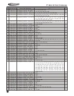
Page 17: ...imeter Test Point PD Adjustm ent Part C117 C52 Require ment 4 2V 0 1V 0 6V 4 2V 0 1V 0 6V Note Adjust ment Watch ing Adjust ment Watch ing Table 6 3 Voltage Controlled Oscillator Table 6 4 Receiver Item Band pass filter Audiopower Sensitivity Squelch activation Test Condition Test frequency intermediate frequency Antenna port input RF OUT 47dBm 1ìV MOD 1kHz DEV 3 0kHz 1 5kHz Audio load 16Ù CH cent...

Page 18: ...djust to 4kHz 2 kHz Adjust to 4kHz 2 kHz Adjust to 0 75kHz 0 35 kHz Adjust to 0 75kHz 0 35 kHz Adjust to 0 75kHz 0 35 kHz Adjust to 0 9kHz 0 45 kHz After adjustment the indicator flashes Note Within 0 2W 200Hz 50Hz Test Point Antenn a Chapter 7 Major Specifications 7 1 General Specification 7 3 Receiver 7 2 Transmitter PT6500 Frenquency range mhz Channel capacity 128 Channel spacing khz Frenquency...

Page 19: ...ce the tube F Frequency Modulation IC4 may be broken replace the IC A Power amplifier tube no power output replace the tube B Replace the microphone if it is broken C Operational Amplifier IC14 may be broken replace it 6 7 Receiving green light is on but no voice is heard Abnormal programmi ng A Replace the speaker if it is broken B Audio power amplifier IC9 may be broken replace it C Switch Tube ...

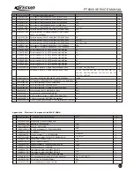
Page 20: ...9 1 25 102 6800CN R01 1 26 201 006500 R01 1 27 204 003208 R02 1 28 204 003208 R07 1 29 121 100000 R17 1 30 204 006200 R09 1 PT6500 SERVICE MANUAL Battery Pack Belt Clip Antenna 31 204 006800 R01 1 32 204 006800 R06 1 33 201 006500 R09 1 34 201 006500 R08 1 35 204 006500 R01 1 36 204 006800 R12 1 37 1 38 201 006500 R06 1 39 203 006500 R02 1 40 203 006500 R04 1 41 202 000558 R08 1 42 302 17040G R01 ...

Page 21: ...0 R02 202 006500 R03 202 006500 R04 202 006500 R05 203 000558 R07B 203 000558 R11 203 006500 R01B 203 006500 R02 203 006500 R03 203 006500 R04 203 006500 R06 203 006500 R07A 203 006800 R26 203 007200 R08 204 006500 R01 204 006500 R02 204 006800 R01 204 006800 R05 204 006800 R06 204 0KB36L R03 301 20020G R01 301 20030G R03 301 20040G R01 301 20080G R02 302 17040G R01 302 20060G R01 304 30040G R02B ...

Page 22: ...s Chip LED 0603 green H19 213SYGC Rohs Chip LED 0603 red 19 21SURC S530 A2 TR8 Rohs Chip triode DTA123JE ROHM Rohs Chip triode DTA143TE Rohs Chip triode DTA144EE ROHM Rohs Chip triode DTC144EE ROHM Rohs Chip triode DTC144EUA ROHM Rohs Chip triode 2SA1586 Rohs Chip triode 2SC3356 R24 Rohs Chip triode 2SC4116 GR Rohs Chip triode 2SC4617 S ROHM Rohs Chip triode 2SC5108Y TOSHIBA Rohs Chip triode KTC40...

Page 23: ...hip resistor 0402 33K 5 Rohs Chip resistor 0402 330K 5 Rohs Chip resistor 0402 360R 5 Rohs Chip resistor 0402 39K 5 Rohs Chip resistor 0402 47R 5 Rohs Chip resistor 0402 470R 5 Rohs Chip resistor 0402 4 7K 5 Rohs Chip resistor 0402 47K 5 Rohs Chip resistor 0402 470K 5 Rohs Chip resistor 0402 5 1K 5 Rohs Chip resistor 0402 51K 5 Rohs Chip resistor 0402 56R 5 Rohs Chip resistor 0402 560R 5 Rohs Chip...

Page 24: ...0 25P 50V C0G Rohs Chip capacitor 0402 20P 5 50V C0G Rohs Chip capacitor 0402 22P 5 50V C0G Rohs Chip capacitor 0402 220P 5 50V C0G Rohs Chip capacitor 0402 2200P 10 50V X7R Rohs Chip capacitor 0402 0 022uF 10 50V X7R Rohs Chip capacitor 0402 0 22uF 10 16V X7R Rohs Chip capacitor 0402 27P 5 50V C0G Rohs Chip capacitor 0402 270P 10 50V X7R Rohs Chip capacitor 0402 33P 5 50V C0G Rohs Chip capacitor ...

Page 25: ... 50V C0G Rohs Chip capacitor 0603 180P 10 50V X7R Rohs Chip capacitor 0603 1P 0 25P 50V C0G Rohs Chip capacitor 0603 22P 5 50V C0G Rohs Chip capacitor 0603 27P 5 50V C0G Rohs Chip capacitor 0603 0 33uF 10 50V X7R Rohs Chip capacitor 0603 39P 5 50V C0G Rohs Chip capacitor 0603 3P 0 25P 50V C0G Rohs Chip capacitor 0603 470P 10 50V X7R Rohs Chip capacitor 0603 4P 0 25P 50V C0G Rohs Chip capacitor 060...

Page 26: ...0805 Rohs Chip bead EMI FILTER SMT BLM11A601S 0603 Rohs Thermistor NTH5G16P42B104K07TH 100K 0603 Rohs Chip transistor NT5032SC 12 8 2 5PPM 5 0 3 2 1 6mm Rohs Chip crystal resonator ZTACC3 58MG Rohs Chip crystal resonator 3 6864MHz Rohs Chip crystal resonator 9 8304MHZ NX5032GA Rohs Chip connector BL112 38RU 38PIN Rohs Chip connector 532680670 6PIN Rohs 2 5mm Earphone connector MOTOROLA Model Rohs ...

Page 27: ...field effect transitor 2SK1824 Chip FET field effect transitor 2SK1829 Chip FET field effect transitor ST2301 Chip touch switch SKRTLBE010 encoder switch RY 6472 Plug in phase frequency detector JTBM450CX24 Plug in porcelain filter LTWC450F 450kHz 7kHz Plug in porcelain filter LTWC450H 450kHz 3kHz chip IF filter DSF753SBF 51 65MHz 4kHz 3dB 7 0x5 0x1 3 mm Chip Resitor 0402 0R 5 Chip Resitor 0402 10...

Page 28: ...02 51K 5 Chip Resitor 0402 56R 5 Chip Resitor 0402 560R 5 Chip Resitor 0402 5 6K 5 Chip Resitor 0402 56K 5 Chip Resitor 0402 560K 5 Chip Resitor 0402 6 8K 5 Chip Resitor 0402 68K 5 Chip Resitor 0402 75K 5 Chip Resitor 0402 82K 5 Chip Resitor 0402 820K 5 Chip Resitor 0603 0R 5 Chip Resitor 0603 10R 5 Chip Resitor 0603 100R 5 Chip Resitor 0603 1K 5 Chip Resitor 0603 100K 5 Chip Resitor 0603 150R 5 C...

Page 29: ... 0 033uF 10 16V X7R Chip Capacitor 0402 3900P 10 50V X7R Chip Capacitor 0402 0 039uF 10 50V X7R Chip Capacitor 0402 3P 0 25P 50V C0G Chip Capacitor 0402 47P 5 50V C0G Chip Capacitor 0402 470P 10 50V X7R Chip Capacitor 0402 0 047uF 10 16V X7R Chip Capacitor 0402 4P 0 25P 50V C0G Chip Capacitor 0402 560P 10 16V X7R Chip Capacitor 0402 5P 0 25P 50V C0G Chip Capacitor 0402 6800P 10 16V X7R Chip Capaci...

Page 30: ...apacitor TS model SIZE A 15uF 20 6 3V Chip trimming capacitor TZV2Z100A110 3 10p 100 Chip inductor LQG11N1R0K00 1uH 0603 0141 05 Chip wire inductor C1608CB 18NJ ceramic core 18NH 5 0603 Chip inductor MLF1608R33K 330nH 10 0603 Chip wire inductor C1608CB 56NJ ceramic core 56nH 5 0603 Chip wire inductor C1608CB 68NJ ceramic core 68nH 5 0603 Chip inductor MLG1608BR10J 100nH 5 0603 Chip inductor MLG160...

Page 31: ... R02 Chip PTT Connector 523650671 6PIN ROHS Chip crystal resonator ZTACC3 58MG Chip crystal resonator 3 6864MHz Chip crystal resonator 9 8304MHZ NX5032GA Chip connector BL112 38RU 38PIN Chip connector 532680670 6PIN 2 5mm Earphone socket MOTOROLA port 3 5mm Mic socket MOTOROLA port PT6500Speaker contact spring SUS301 wire 0 3mm gilt Voice recorder IC W588A080 binding W588PCB PT558 Voice recorder I...

Page 32: ...e Specification Accessories Battery Li Poly battery Hanging loop Earphone Charger 7 hour standard charger Antenna long antenna Short antenna KB 36C 7 4V 1750mAH KGS 03 KME 014 KME 015 KME 016 KBC 36C Belt Clip KBJ 04 PT6500 SERVICE MANUAL ...

Page 33: ...PT6500 SERVICE MANUAL Figure 1 PT6500 Top Main Board Position Number Diagram 136 174MHz 32 ...

Page 34: ...PT6500 SERVICE MANUAL Figure2 PT6500 Bottom Main Board Position Number Diagram 136 174MHz 33 ...

Page 35: ...Figure 3 400 470MHz PT6500 Top Main Board Position Number Diagram 34 PT6500 SERVICE MANUAL ...

Page 36: ...35 PT6500 SERVICE MANUAL Figure 4 400 470MHz PT6500 Bottom Main Board Position Number Diagram ...

Page 37: ...Figure 5 PT6500 PTT Top Board Position Number Diagram 36 PT6500 SERVICE MANUAL ...

Page 38: ...37 PT6500 SERVICE MANUAL Figure 6 PT6500 PTT BOTTOM Board Position Number Diagram ...

Page 39: ...38 PT6500 SERVICE MANUAL Figure 7 PT6500 Top Keyboard Schematic Circuit Diagram Figure 8 PT6500 Bottom Keyboard Schematic Circuit Diagram ...
Page 40: ...T 14 DVDD 15 Vp 16 IC2 ADF4111 R48 4 7K C84 101 R43 560R C96 0 1uF 35V R44 560R R45 2 7K C112 1uF 16V R41 560R C102 0 1uF 35V R46 2 7K C118 1uF 16V L33 BLM11A221S C20 4 7uF 10V C33 104 L9 BLM11A221S C21 471 R2 10R R24 2 7K C61 R47 10R C110 471 C122 4 7uF 10V C115 103 C114 104 L34 BLM11A221S C113 471 R49 10R C109 471 D10 MA2S111 R40 1K R42 150K C95 103 C106 101 C105 101 C104 101 Q13 DTC144EE C133 4...

Page 41: ...9 105 C307 4 7uF 10V C344 4 7uF 10V C306 471 C329 471 Q44 DTA123JE Q39 ST2301 Q43 ST2301 C305 4 7uF 10V C317 4 7uF 10V C311 471 C323 471 C336 4 7uF 10V C335 471 Rset 1 CP 2 CPGND 3 AGND 4 RFinB 5 RFinA 6 AVDD 7 REFin 8 DGND 9 CE 10 CLK 11 DATA 12 LE 13 MUXOUT 14 DVDD 15 Vp 16 IC2 ADF4111 R48 4 7K C84 101 R43 560R C96 0 1uF 35V R44 560R R45 2 7K C112 1uF 16V R41 560R C102 0 1uF 35V R46 2 7K C118 1u...

Page 42: ...1 BLM11A601S C150 102 R69 10R VC 1 GND 2 VCC 4 OUT 3 X1 12 8MHz L42 4 7uH C142 10P C143 10P R54 0R C119 102 R68 47R C128 47P C155 18P Q15 KTC4082 R61 330K L44 100nH C146 102 R77 2 2K L45 100nH C136 102 C144 100P L35 100nH C121 101 D14 1SV325 D11 1SV325 C108 6P L36 22nH Q11 2SK508NV K52 C123 3 5P C124 3P C103 5P L37 3 3uH R52 180R C107 0 5P R39 100R L31 220nH C101 120P C116 L38 220nH C117 10P D12 D...

Page 43: ...O A F C D D E T S 7 X 9 8 3 0 S W P O W Q 4 S A D F 4 M O Q R F P A P 5 4 5 0 M U T D A 8 S C S D A B U S Q 3 S W 5 8 5 1 2 8 X T C I C W 5 8 8 5 T V C Q 1 R 5 Q 1 4 2 N D L S C F 4 5 0 I C A K 2 p i n p i n M O p i n Q 3 H Q 3 H I C H A M I C I C H T 9 I C I C I C I C A M L L A M p i n T X C T C S S D T 2 M I C I C 1 A M I C 1 Q 4 S M U M I R X V O p i n 5 5 R Q 3 S 5 S A Q 4 S 5 X C 6 2 0 4 Q 4 ...

Page 44: ...18 19 20 21 22 23 24 39 25 26 27 28 29 30 31 32 33 34 35 36 37 38 CN3 CN38 C11 221 C7 221 C6 221 1 2 3 4 5 6 7 8 9 10 11 12 13 14 15 CN1 CN14 L1 BLM11A221S C13 103 C12 102 R4 0R R8 R7 2 7K R6 2 7K R3 2 7K R2 2 7K R1 2 7K L2 BLM11A221S C15 103 C14 102 按键板电原理图 名称 文件号 设计 批准 机型 版本 审核 第 张 张 共 PT6500 KEY 集群 1 1 Q3 2SK1824 R23 R21 100K R5 2 7K C1 221 C2 221 C23 221 C24 221 C25 221 C26 221 C27 221 C28 221...

Page 45: ...1 1 2 2 3 3 4 4 D D C C B B A A 1 2 3 4 5 6 7 CN1 CN6 SW1 SW2 SW3 R1 20K R2 4 7K 电原理图 名称 文件号 设计 批准 机型 版本 审核 第 张 张 共 PT6500 PTT 1 1 Figure 13 PT6500 PTT Board Schematic Circuit Diagram ...
Page 46: ...L1 1uH L2 1uH L3 0140 05 t TH1 10k C1 1000p Charger T Charger BAT BAT D1 1N5819 2 2k CN1 LTP190 PDF created with pdfFactory Pro trial version www pdffactory com Figure 14 KB 36C ...

Page 47: ... R1 4 7K 1 C6 104 C11 104 R9 100k D3 IN4148 D4 IN4148 B B C4 470P R12 1k D6 IN4148 5V C16 470P R17 82K C117 102 C18 104 D5 IN4148 R19 100R R18 NC R20 10K C19 104 C21 104 C20 104 R25 470R R14 470R R21 470R R23 470R R22 470R R26 0 L2 L C22 470P C25 102 C24 102 C23 102 DETC DETC B TEMP B TEMP C28 10uF 25V J2 J3 J4 J5 L1 330uH 3A 5V 5V C17 47uF 25V C3 10uF 25V C1 0 1uF D11 IN5819 D12 IN4148 C5 470P R1...

Reviews: