PW-A
17
CIRCUIT DESCRIPTION
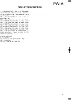
outputs a "/BACK" signal.
3. ROM and RAM These ROM and RAM are connected
with the CPU. The ROM is a socket type and the
program differs with the models.
4. USB control circuit This circuit executes communica-
tion through the USB interface and sends data to the
CPU. It has IC4 for controlling the USB, X1 for
generating 48 MHz clock pulses, IC14 for producing 3.3
V. and USB connector J5. It is installed in the GU and
USB.
5. GP-IB control circuit This circuit executes communi-
cation through the GP-IB and sends data to the CPU.
It has IC10 exclusive for GP-IB control, line driver IC11
and IC12, and GP-IB connector J1. It is installed in
the GU.
6. Local bus control circuit
This circuit connects PW-
A power supply units with the GU and/or USB units
installed with each other. It consists of a line driver
IC13, terminator resistors R35 and R36, and selector
switch S1.
7. RS-232C and local bus control circuit
These are the
RS-232C interface and the local bus control circuit with
a modular jack. They consist of a line driver IC18 and
Q1, 2 and 3.
8. ROM socket When ROM is installed on this socket
and R6 is short-circuited, the unit may be started using
the ROM program. When the exclusive copy program is
stored in the ROM
shown
in
3,
the program in this ROM
may be written in the ROM in the power supply unit.
INPUT UNIT
(X72-162)
The optional X72-1620-** input unit enables the output
voltage to be reduced quickly when no load or a low
load is connected.
It has constant-current discharging circuit for each
channel and discharges the capacitors at the output
end.
This unit is connected with an amplifier unit and is
connected with the output end from there. It receives
the output signal of the CV amplifier of each channel
from the amplifier unit and operates only when the
output is off.
The mounted parts differ with the number of channels,
output voltages and polarity. There are eight
modifications in all.
AMP UNIT (X73-232)
The amplifier unit controls DC current input from the
power supply unit C/6 to the set value sent by the CPU
unit.
The DAC converts serial data of the set value sent by
the CPU unit into analog data. The amplifier unit
compares these analog data with the monitored value
and controls the DC current.
Each of four channels has the same circuit
configuration. However, different parts are used
according to the output voltage and current and their
Channels 2 and 4 use the COM commonly. In a three-
channel power supply unit, channels 1 and 2 use a
different common line from channel 3. Thus, the power
lines are different.
Since the circuit configuration is identical, the
description below explains channel 1.
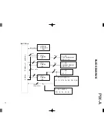
(A number is a number of a block diagram)
1. D/A converter (IC2) (CH2: IC1, CH3: IC20, CH4:
IC19)
The D/A converter receives digital signal
indicating the set value from the CPU unit and converts
it into an analog signal. The PCM1700U, a DAC unit
used, has two circuits, which convert the CVREF
voltage and CCREF voltage, respectively.
The D/A converter outputs approximately 0 to -2.25 V
through pins 16 and 27, regardless of the output on/off
condition.
2. REF (non) reversing circuit (IC3 and IC4)
This
circuit amplifies the output voltage of the D/A converter
by reversing or not reversing it according to its polarity.
Channel 1 uses all of 00 to 09 as two reversing
amplifiers to provide non-reverse output. CV REF is
output through pin 1, and CC REF is output through pin
7. The voltage is
approximately 0 to -7.5 V.
3. CC error amplifier (IC8-1/2)
This amplifier compares the CC REF output (B) of the
REF (non) reversing circuit with the output (D) of the
current detector circuit and amplifiers the error to
control the power transistors in CC operation.
4. CV error amplifier (IC8-2/2)
This amplifier compares the output (C) of the REF (non)
reversing circuit with the output voltage sensing value
(E) and amplifiers the error to control the power
transistors in CV operation.
This amplifier ORs the
outputs shown in 3 and 4 and always use either output
to control the power transistors shown in 5 below.
5. Power transistors (First stage: Q4, 5 and 6, final
stage: Q1, 2 and 3) (CH2 … First stage: Q10, 11 and
12, final stage: Q7, 8 and 9. CH3 … First stage: Q15
and 16, final stage: Q13 and 14. CH4 … First stage:
Q19 and 20, final stage: Q17 and 18.)
These are the main power transistors for stabilizing the
output power. Two transistors are Darlington- connected.
The number and characteristics of the power transistors
differ with the output specifications.
6. Current detection circuit (R41 and IC11)
The four-
terminal resistor R41 detects the output current, which
is input to the differential amplifier (IC11 1/2), reversed
by a buffer and input into the CC error amplifier shown
in 3.
Since the
voltage must be positive when monitoring
the current, positive power does not pass through the
reversing buffer and is
input
to the
signal selector shown
in 9.
Negative power is
reversed
by the reversing buffer.
7.
Volt age monitor circuit (IC10 2/2)
This circuit attenuates the output voltage A and
produces a voltage monitoring signal.
8.
OUT ON/OFF (Q21 OR Q22)
This circuit makes the base signal of the
power
polarity. In particular, the power transistors are quite
different. In a three-channel power supply unit, Q13 to
Q20 are used for channel 3.
transistors and CV/CC REF into positive or negative
voltage according to the CPU and stops the output.
Parts and voltage differ with the polarity of the output.
Summary of Contents for PW-A series
Page 57: ...A C E G I B D F H J SCHEMATIC DIAGRAM PW A ...
Page 58: ...SCHEMATIC DIAGRAM L N P R T M O Q S PW A ...
Page 59: ...SCHEMATIC DIAGRAM U W Y AA AC V X Z AB AD PW A ...
Page 60: ...AF AH AJ AL AN AG AI AK AM SCHEMATIC DIAGRAM PW A ...
Page 61: ...AO AQ AS AU AW AP AR AT AV AX SCHEMATIC DIAGRAM PW A ...
Page 62: ...PW A Y39 4160 00 AY BA BC AZ BB ...
Page 63: ...BE BG BI BK BM BF BH BJ BL SCHEMATIC DIAGRAM PW A ...
Page 64: ...BN BP BR BT BV BO BQ BS BU BW SCHEMATIC DIAGRAM PW A ...

