


PW-A
8
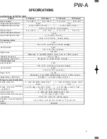
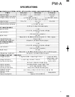
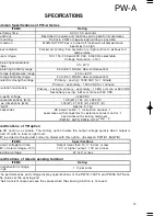
SPECIFICATIONS
Speci f i cat i ons of PW 18- 2 ATP
ITEMS
0 t o +3 6 V
0 t o +1 8 V
0 t o +8 V
10 m V
1 m V
±
±
O u tp ut c u r r e nt
±
1 m V
2 mV
0.5 m V
50
µ
s ( t yp . )
2 m A
5 m A
( F o r 0 t o 10 0% va r iat io n )
1.5 m A
In dependent
Channel
A
Channel
B
Channel
C
Output voltage
Voltage setting resolution
Voltage setting accuracy
Current setting resolution
Current setting accuracy
CV characteristics
CC characteristics
T r ans ient re s p o n s e
T e mper ature c oef f ic ie n t
T e mper ature c oef f ic ie n t
Load variation
Input variation
Load variation
Input variation
Ripple noise
Ripple noise
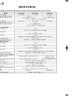
Current indicator
Voltage indicator
Voltage & current indication
Current indication accuracy &
resolution
Current indication accuracy &
resolution
Voltage
range
current indication
&
Common
Common
Power consumption
Approx. 191W, 242 VA
(0.5% SET +5mV)
(0.5% SET +20mV)
At 23
±
5
after 30 - minute aging
At 23
±
5
after 30 - minute aging
1 mA
(1% SET +5mA)
0 to +1A
0 to +2A
0 to +2A
(Fo r
±
10% va r i at ion of source voltage)
(Fo r
±
10% va r iat i on of source voltage)
(For 0 to 100% variation)
Measured in the RMS method using 5 Hz to 1 MHz signals.
Measured in the RMS method using 5 Hz to 1 MHz signals.
60 ppm/
( at rated output voltage)
150 ppm/
( at rated output current)
4 - digit red LEDs, lowest digit: 1mA
4 - digit red LEDs, lowest digit: 10mV
4 - digit red LEDs,
lowest digit: 1mV
±
( 0. 5% rdg + 20 mV ) /10mV
±
( 0. 5% rdg + 5 mV )/1mV
At 23
±
5
after 30 - minute aging
At 23
±
5
after 30 - minute aging
±
(1% rdg + 5mA)/ 1mA
-2.5% FS to + 102.5% FS/0% FS to + 102.5% FS
ı
ı
ı
ı
ı
ı
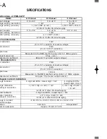
Summary of Contents for PW-A series
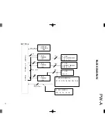
Page 57: ...A C E G I B D F H J SCHEMATIC DIAGRAM PW A ...
Page 58: ...SCHEMATIC DIAGRAM L N P R T M O Q S PW A ...
Page 59: ...SCHEMATIC DIAGRAM U W Y AA AC V X Z AB AD PW A ...
Page 60: ...AF AH AJ AL AN AG AI AK AM SCHEMATIC DIAGRAM PW A ...
Page 61: ...AO AQ AS AU AW AP AR AT AV AX SCHEMATIC DIAGRAM PW A ...
Page 62: ...PW A Y39 4160 00 AY BA BC AZ BB ...
Page 63: ...BE BG BI BK BM BF BH BJ BL SCHEMATIC DIAGRAM PW A ...
Page 64: ...BN BP BR BT BV BO BQ BS BU BW SCHEMATIC DIAGRAM PW A ...


