1-8 (No.RA012<Rev.001>)
2.3.3.3
APC Circuit
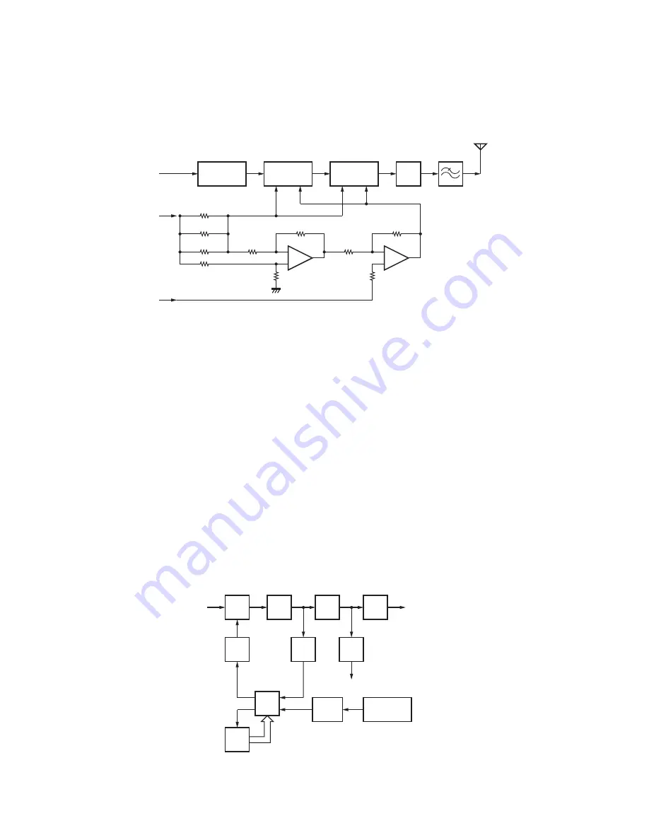
The APC circuit always monitors the current flowing through the drive amplifier (Q206) and RF power amplifier (Q208), and keeps it
constant. The voltage drop at R230, R231 and R233 is caused by the current flowing through the RF final amplifier. This voltage is
applied to the differential amplifier IC200 (1/2).
IC200 (2/2) compares the output voltage of IC200 (1/2) with the reference voltage from IC705 (32pin:AUXDAC1). The output of IC200
(2/2) controls the gate bias voltage of the RF power amplifier and the drive amplifier to make both voltages the same.
The change of power (high/low) is carried out by the change of the reference voltage.
Fig.5 Drive and final amplifier and APC circuit
2.3.4 Frequency Synthesizer Unit
2.3.4.1
Frequency synthesizer
The frequency synthesizer consists of the TCXO (X1), VCO, PLL-IC (IC2), and buffer amplifiers.
The TCXO generates 16.8MHz. The frequency stability of TCXO is 0.5ppm within the temperature range of -30
°
C to +60
°
C. The fre-
quency tuning and modulation of the TCXO are done to apply voltage to pin 1 of the TCXO. The TCXO output is applied to pin 10 of
the PLL-IC.
The VCO consists of 2 VCOs and covers a dual range of 396.05625~396.246875MHz and 446.00625~446.196875MHz. The VCO
generates 396.05625~396.246875MHz to provide the first local signal for reception. The operating frequency is generated by Q6 in
transmitting mode and Q5 in receiving mode. The oscillation frequency is controlled by applying the VCO control voltage, obtained
from the phase comparator (IC2) to the variable capacitance diodes (D5, D9, D11,and D13 while transmitting and D4, D7 and D12
while receiving).
The TX/RX pin of IC710 goes “high” in transmission mode, causing Q8 to turn off, and Q7 turn on. The TX/RX pin goes “low” in recep-
tion mode.
The output from Q5 and Q6 are amplified by a buffer amplifier (Q9) and RF amplifier (Q2), and are then sent to the PLL-IC. The PLL-
IC consists of a prescaler, reference divider, phase comparator, and charge pump.
The input signal from pin 10 and 17 of the PLL-IC is divided down and compared at the phase comparator. The pulse output signal of
the phase comparator is applied to the charge pump and transformed into a DC signal in the loop filter (LPF). The DC signal is applied
to the CV of the VCO and is locked to keep the VCO frequency constant.
PLL data is output from PLL_LE (pin 87), PLL_DATA (pin 86) and PLL_CLK (pin 88) of the MCU (IC710). The data is input to the PLL-
IC when the channel is changed or when transmission is changed to reception and vice-versa. The PLL lock condition is always mon-
itored by pin 70 (PLL_LD) of the MCU. When the PLL is unlocked, PLL_LD goes low.
Fig.6 PLL block diagram
ANT
RF FINAL
AMP
ANT
SW
From
T/R SW
(D15)
D203,204
+B
PC
Q208
DRIVE
AMP
Q206
VDD
VG
Pre-DRIVE
AMP
Q201
IC200
(1/2)
IC200
(2/2)
R230
R231
R233
BUFF
Baseband
VCO
PLL
MCU
IC710
PLL_LE,PLL_DATA,PLL_CLK
IC2
PLL_LD
17
10
21
7
BUFF
SW
LPF
To mixer
VC
Q10
RF
AMP
Q9
TCXO
X1
IC705
SW
To
RF AMP
TX/RX
(TX: High)
D15
D14
Q2
CV


