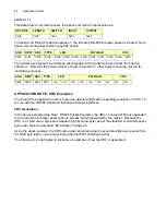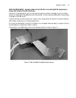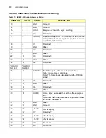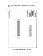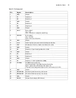
SK/SP to SKB Pinout comparison and Harness Wiring
Table 12: SKB II to SK Adapter Harness Wiring
SKB II PIN
SK PIN
SIGNAL
DESCRIPTION
13
1
GND
Ground
14
2
GND
Ground
15
3
BUSY
Busy output: low=idle, high= switching
16
4
D0
Data line 0
17
5
ERROR
Reset error output low = normal, high = switch mecha-
nism position check failed (channel position is verified
when SK switch is reset)
18
6
D1
Data line 1
19
7
GND
Shield
20
8
D2
Data line 2
21
9
GND
Shield
22
10
D3
Data line 3
23
11
GND
Shield
24
12
D4
Data line 4
POLARIZ-
ING KEY
POLARIZ-
ING KEY
25
13
/STROBE
/STROBE input, active low = read data lines;
high = ignore state of data lines.
Note: The home line is also read in via the STROBE
signal
26
14
D5
Data line 5
27
15
GND
Shield
28
16
D6
Data line 6
29
17
GND
Shield
30
18
/HOME
Home input: low sends the switch to the home posi-
tion.
Note: the state of the /Home line is only checked when
the strobe line is active.
31
19
GND
Shield
32
20
GND
Ground
33
21
+5 VDC
+5 volt supply
1
34
22
D7
Data line 7
35
23
+5 VDC
+5 volt supply
1
36
24
+5 VDC
+5 volt supply
1
37
25
NC
No connect
38
26
NC
No connect
Summary of Contents for SKB Series
Page 1: ...SKB SERIES FIBEROPTIC SWITCH MODULE User Manual ...
Page 2: ...ii 10109002 Rev 001 August 2001 2001 JDS Uniphase All rights reserved ...
Page 4: ...iv ...
Page 11: ...7 Contents ...
Page 13: ...9 List of Figures ...
Page 15: ...11 List of Tables ...
Page 19: ...4 Safety Information Instructions and Symbols ...
Page 25: ...10 Introduction ...
Page 53: ...38 Operation and Control Instructions ...
Page 91: ...76 Commands ...
Page 111: ...96 Application Notes ...
Page 113: ...98 Service ...


