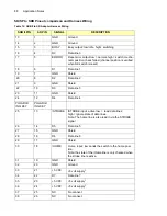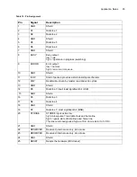
Table 15: Pin Assignment
Pin
Signal
Description
1
GND
Shield
2
D1
Data line 1
3
D2
Data line 2
4
GND
Shield
5
D5
Data line 5
6
D6
Data line 6
7
GND
Shield
8
BUSY
Busy output:
low = idle
high = operation in progress (switching)
9
ERROR
Error output:
low = normal
high = error in error queue
10
GND
Shield
11
/SOP
Start of packet--provides a start-and-stop mechanism
12
R/W
Read/write--driven by master read and write cycles
13
GND
Shield
14
D0
Data line 0 input; least significant bit (LSB)
15
GND
Shield
16
D3
Data line 3
17
D4
Data line 4
18
GND
Shield
19
D7
Data line 7; most significant bit (MSB)
20
STROBE
STROBE input, active low:
high-to-low pulse = read data lines and home line
high = ignore state of data lines and home line
This line is internally pulled high via 10 K ohm resistor to 5 V DC
21
GND
Shield
22
RESERVED
Reserved; internal use only; do not use
23
RESERVED
Reserved; internal use only; do not use
24
GND
Shield
25
RESET
Resets the hardware (MCU reset)
Summary of Contents for SKB Series
Page 1: ...SKB SERIES FIBEROPTIC SWITCH MODULE User Manual ...
Page 2: ...ii 10109002 Rev 001 August 2001 2001 JDS Uniphase All rights reserved ...
Page 4: ...iv ...
Page 11: ...7 Contents ...
Page 13: ...9 List of Figures ...
Page 15: ...11 List of Tables ...
Page 19: ...4 Safety Information Instructions and Symbols ...
Page 25: ...10 Introduction ...
Page 53: ...38 Operation and Control Instructions ...
Page 91: ...76 Commands ...
Page 111: ...96 Application Notes ...
Page 113: ...98 Service ...


