background image

Quasi-resonant CoolSET design guide

ICE2QRxx65/80x

Design Guide

7

8 August 2011

85 ~ 265 VAC

Snubber

C

bus

D

r1

~D

r4

R

CS

TL431

Optocoupler

R

b1

R

b2

R

c1

C

c1

C

c2

R

ovs2

R

ovs1

C

VCC

D

VCC

D

O

C

O

L

f

C

f

V

O

C

PS

Startup Cell

CoolSET

®

-Q1

CoolMOS

®

W

p

W

s

W

a

R

VCC

C

ZC

R

ZC2

R

ZC1

Drain

Zero Crossing Block

Power Management

Cycle-by-Cycle

current limitation

Active Burst Mode

PWM controller

Current Mode Control

Protections

VCC

CS

Control Unit

ZC

FB

GND

Figure 2 Typical Application of ICE2QRxx65/80x

The drain-source voltage of the power switch V

ds

will rise very fast after MOSFET is turned off. This is caused

by the energy stored in the leakage inductance of the transformer. A snubber circuit, RCD in most cases, can
be used to limit the maximum drain source voltage caused. After the oscillation 1, the drain-source voltage
goes to its steady value. Here, the voltage v

Refl

is the reflected value of the secondary voltage at the primary

side of the transformer and is calculated as:

n

V

V

V

do

out

Refl

(1)

where n the turns ratio of the transformer, which is defined in this document as:

P

S

/N

N

n

(2)

with N

p

and N

s

are the turns count of the primary and secondary winding, respectively.

After the oscillation 1 is damped, the drain-source voltage of the power switch shows a constant value of
V

bus

+V

Refl

until the transformer is fully demagnetized. This duration builds up the first portion of the off-time

t

off1

.

After the secondary side current falls to zero, the drains-source voltage of the power switch shows another
oscillation (oscillation 2 in Figure 3, this is also mentioned as the main oscillation in this document). This
oscillation happens in the circuit consisting of the equivalent main inductance of the transformer L

p

and the

capacitor across the drain-source (or drain-ground) terminal C

DS

which includes C

o(er)

of the MOSFET. The

frequency of this oscillation is calculated as:

DS

P

OSC2

C

L

1

f

(3)

The amplitude of this oscillation begins with a value of v

Refl

and decreases exponentially with the elapsing

time, which is determined by the losses factor of the resonant circuit. The first minimum of the drain voltage
appears at the half of the oscillation period after the time t

4

and can be apporximated as:

Refl

bus

dsMin

V

-

V

V

(4)

In the quasi-resonant control, the power switch is switched on at the minimum of the drain-source voltage.
From this kind of operation, the switching-on losses are minimized, and switching noise due to dV

ds

/dt is

reduced compared to a normal hard-switching flyback converter.

Summary of Contents for CoolSET ICE2QR 65 Series

Page 1: ...Design Guide Version 1 1 8 August 2011 N e v e r s t o p t h i n k i n g Power Management Supply ICE2QRxx65 80x Q u a s i R e s o n a n c e C o o l S E T D e s i g n G u i d e AN PS0053 ...

Page 2: ... and conditions and prices please contact the nearest Infineon Technologies Office www infineon com Warnings Due to technical requirements components may contain dangerous substances For information on the types in question please contact the nearest Infineon Technologies Office Infineon Technologies components may be used in life support devices or systems only with the express written approval o...

Page 3: ... typo ICE2QRxx65 80x Quasi Resonance CoolSET Design Guide License to Infineon Technologies Asia Pacific Pte Ltd AN PS0053 Winson Wong Winson wong infineon com Eric Kok Eric kok infineon com We Listen to Your Comments Any information within this document that you feel is wrong unclear or missing at all Your feedback will help us to continuously improve the quality of this document Please send your ...

Page 4: ...C Pre Charging and Typical VCC Voltage During Start up 8 4 1 1 VCC Capacitor 9 4 2 Soft Start 9 4 3 Normal Operation 10 4 3 1 Switch on Determination 10 4 3 2 Switch off Determination 11 4 4 Active Burst Mode Operation 11 4 4 1 Entering Active Burst Mode Operation 11 4 4 2 During Burst Mode Operation 12 4 4 3 Leaving Active Burst Mode 13 4 5 Current sense 13 4 6 Feedback 13 4 7 Zero crossing 13 4 ...

Page 5: ...de operation and low output voltage ripple The numerous protection functions give a full protection of the power supply system in failure situation All of these make the ICE2QRxx65 80x an outstanding power CoolSET for quasi resonant flyback converter in the market In addition numerous protection functions have been implemented in the CoolSET to protect the system and customize the CoolSET for the ...

Page 6: ... Drain This pin is connected to the drain of the 650V 800V CoolMOS 2 3 5 VCC Power supply The VCC pin is the positive supply of the CoolSET and should be connected to auxiliary winding of the main transformer 2 3 6 GND Ground This is the common ground of the CoolSET Note that the current sense resistor ground should be connected to bulk capacitor ground in order to avoid strong noise interruption ...

Page 7: ...ng respectively After the oscillation 1 is damped the drain source voltage of the power switch shows a constant value of Vbus VRefl until the transformer is fully demagnetized This duration builds up the first portion of the off time toff1 After the secondary side current falls to zero the drains source voltage of the power switch shows another oscillation oscillation 2 in Figure 3 this is also me...

Page 8: ...oltage device provides a current to charge the VCC capacitor Cvcc Before the VCC voltage reaches a certain value the amplitude of the current through the high voltage device is only determined by its channel resistance and can be as high as several mA After the VCC voltage rises to certain level the CoolSET controls the startup cell so that a constant current around 1mA is provided to charge the V...

Page 9: ... there is a VCC undervoltage protection the capacitance of the VCC capacitor should be selected to be high enough to ensure that enough energy is stored in the VCC capacitor so that the VCC voltage will never touch the VCC under voltage protection threshold VVCCUVP before the output voltage is built up Therefore the capacitance should fulfill the following requirement VCCUVP VCCon 1 2 VCCop VCC V ...

Page 10: ... The up down counter stores the number of zero crossing to be detected to switch on the main power switch after demagnetisation of the transformer This value is a function of the feedback voltage VFB which contains information about the output power Generally a high output power results in a high feedback voltage VFB According to this information the value in the up down counter is changed to a lo...

Page 11: ...mode operation the digital comparator is disabled and no pulse will be generated 4 3 2 Switch off Determination In the converter system the primary current is sensed by an external shunt resistor which is connected between Current Sense pin and the common ground The sensed voltage across the shunt resistor VCS is applied to an internal current measurement unit and its output voltage V1 is compared...

Page 12: ...mode operation only when the output power is really low during the preset blanking time 4 4 2 During Burst Mode Operation After entering the Active Burst Mode the feedback voltage rises as VO starts to decrease due to the inactive PWM section One comparator observes the feedback signal if the voltage level VBH 3 6V is exceeded In that case the internal circuit is again activated by the internal bi...

Page 13: ... voltage VCS_PK is 1V Therefore the current sense resistor can be chosen according to the maximum required peak current in the transformer as shown in 9 p pk CS I R _ 1 9 The design procedure of quasi resonant flyback transformer is shown in 2 In addition a leading edge blanking LEB is already built inside the current sense pin The typical value of leading edge blanking time is 330ns which can be ...

Page 14: ...herefore the current flowing out from ZC pin at this moment is P ZC a BUS ON ZC N R N V I 1 _ 12 The threshold in ZC pin to start the foldback point correction is IZC 0 5 mA Therefore RZC1 can be chosen so that P a S BUS ZC N mA N V R 5 0 _ 1 13 In 13 VBUS_S is the voltage from which the maximum output power is desired to be maintained at constant level The corresponding maximum current sense volt...

Page 15: ...ge is higher than the preset threshold VZCOVP the CoolSET is latched off after the preset blanking time If the junction temperature of CoolSET exceeds 140o C the CoolSET enters into auto restart mode If the voltage at the current sensing pin is higher than the preset threshold VCSSW during on time of the power switch the CoolSET is latched off This is short winding protection During latch off prot...

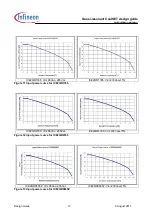
Page 16: ...ifier loss and the MOSFET power loss are considered The only information needed is the required output power the input voltage range the operating ambient temperature and the efficiency of the system The required input power can then be calculated as equation 14 o in P P 14 where Pin input power Po output power η efficiency It then simply looks up the closed input power at the required ambient tem...

Page 17: ...QR1765 Vin 85Vac 265Vac ICE2QR1765 Vin 230Vac 15 Figure 11 Input power curve for ICE2QR1765 ICE2QR4765 Vin 85Vac 265Vac ICE2QR4765 Vin 230Vac 15 Figure 12 Input power curve for ICE2QR4765 ICE2QR0665Z Vin 85Vac 265Vac ICE2QR0665Z Vin 230Vac 15 Figure 13 Input power curve for ICE2QR0665Z ...

Page 18: ...1065Z Vin 85Vac 265Vac ICE2QR1065Z Vin 230Vac 15 Figure 14 Input power curve for ICE2QR1065Z ICE2QR1765Z Vin 85Vac 265Vac ICE2QR175Z Vin 230Vac 15 Figure 15 Input power curve for ICE2QR1765Z ICE2QR4765Z Vin 85Vac 265Vac ICE2QR4765Z Vin 230Vac 15 Figure 16 Input power curve for ICE2QR4765Z ...

Page 19: ...665G Vin 85Vac 265Vac ICE2QR0665G Vin 230Vac 15 Figure 17 Input power curve for ICE2QR0665G ICE2QR1765G Vin 85Vac 265Vac ICE2QR1765G Vin 230Vac 15 Figure 18 Input power curve for ICE2QR1765G ICE2QR4765G Vin 85Vac 265Vac ICE2QR4765G Vin 230Vac 15 Figure 19 Input power curve for ICE2QR4765G ...

Page 20: ...680Z Vin 85Vac 265Vac ICE2QR0680Z Vin 230Vac 15 Figure 20 Input power curve for ICE2QR0680Z ICE2QR2280Z Vin 85Vac 265Vac ICE2QR2280Z Vin 230Vac 15 Figure 21 Input power curve for ICE2QR2280Z ICE2QR4780Z Vin 85Vac 265Vac ICE2QR4780Z Vin 230Vac 15 Figure 22 Input power curve for ICE2QR4780Z ...

Page 21: ...W for 650V DIP 7 CoolSET there is no copper area as heatsink and the Rthja 96K W for 650V DSO 12 CoolSET there is no copper area as heatsink and the Rthja 110K W for 800V DIP 7 CoolSET there is 232mm2 copper area of 2oz PCB at drain pin for heatsink and the Rthja 80K W and for 800V DSO12 CoolSET there is 232mm2 copper area of 2oz PCB at drain pin for heatsink and the Rthja 85K W 4 Saturation curre...

Page 22: ...filter return ground Y capacitor C15 auxiliary winding ground of transformer and the RCS resistor The high voltage pins are connected to bus voltage in typical applications During lightning surge test the noise on bus voltage is high It is suggested that the track to high voltage pin shall be kept away from other small signal tracks The distance is better to be more than 3mm 8 Product Portfolio Qu...

Page 23: ...N p s Auxiliary turns s diode out diode cc aux N V V V V N ICE2QRxx65 80x external component design Current sense resistor P pk CSth CS I V R _ VCC capacitor VCCon e VCCch startup VCC V I t C 2 arg tstartup startup time of system suggested CVCC is 22μF ZC resistors p aux S BUS ZC N mA N V R 5 0 _ 1 1 _ 1 2 ZCOVP diode OVP out s aux ZC ZC V V V N N R R Vout_OVP output OVP voltage VBUS_S bulk capaci...

Page 24: ...8 Infineon Technologies 12 Datasheet ICE2QR0680Z Off Line SMPS Quasi Resonant PWM Controller with integrated 800V Startup Cell Depletion CoolMOS In DIP7 Infineon Technologies 13 Datasheet ICE2QR2280Z Off Line SMPS Quasi Resonant PWM Controller with integrated 800V Startup Cell Depletion CoolMOS In DIP7 Infineon Technologies 14 Datasheet ICE2QR4780Z Off Line SMPS Quasi Resonant PWM Controller with ...

Reviews: