


Application Note
10 of 27
V 1.0
2021-04-30
CoolGaN™ IPS half-bridge evaluation board with IGI60F1414A1L
Setup and use
4.2.1
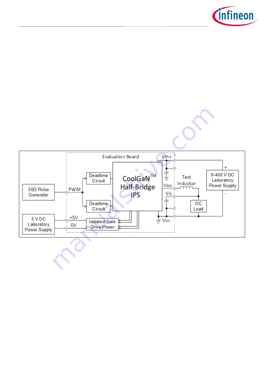
Connections for double-pulse testing
shows a proper setup and connections for double-pulse testing. Terminal X1 has all 6 output power
connections. 5 V DC supply connection is provided in this terminal. The inductor also connects to the terminal
block. The inductor energy is dissipated in the freewheeling transistor; therefore, there is no need for external
load. For double pulse testing refer to section 4.8 in reference [1].
4.2.2
Connections for buck topology
shows the setup in buck topology configuration. Connect the external inductor between the DC load
and the half-bridge output terminal (V
sw
) and the V
o
terminal
.
DC load connects to V
o
. The output voltage is
proportional to the duty cycle of the PWM applied to the J1. If a resistive load is applied and the inductor
current is above the boundary condition (continuous current mode) then the high-side will turn-on in a hard
switching condition. Therefore, select a proper switching frequency (<150 kHz), duty cycle (<75 percent), and
load value (>100 ohm).
Attention:
It is recommended to monitor the temperature of the IPS chipset to not exceed T
c
=125°C.
Figure 10
Connecting the evaluation board in the buck topology
4.2.3
Connections for boost topology
In the boost topology (shown in
V
o
is the input source and V
in+
is the output terminal. This setup will
provide a boost testing hardware and the DC bus value and the duty cycle has to be carefully selected to ensure
the output voltage will not exceed 450 V rating of the capacitors.
Attention:
There is no closed loop control in the boost condition and losing the DC load will result in
charging the output capacitors rapidly and will result in a catastrophic failure. All safety
measures must be considered setting up a boost topology.