IEI Technology WAFER-945GSELVDS2-N270-R10 User Manual Download Page 72


WAFER-945GSELVDS2

Page 60 


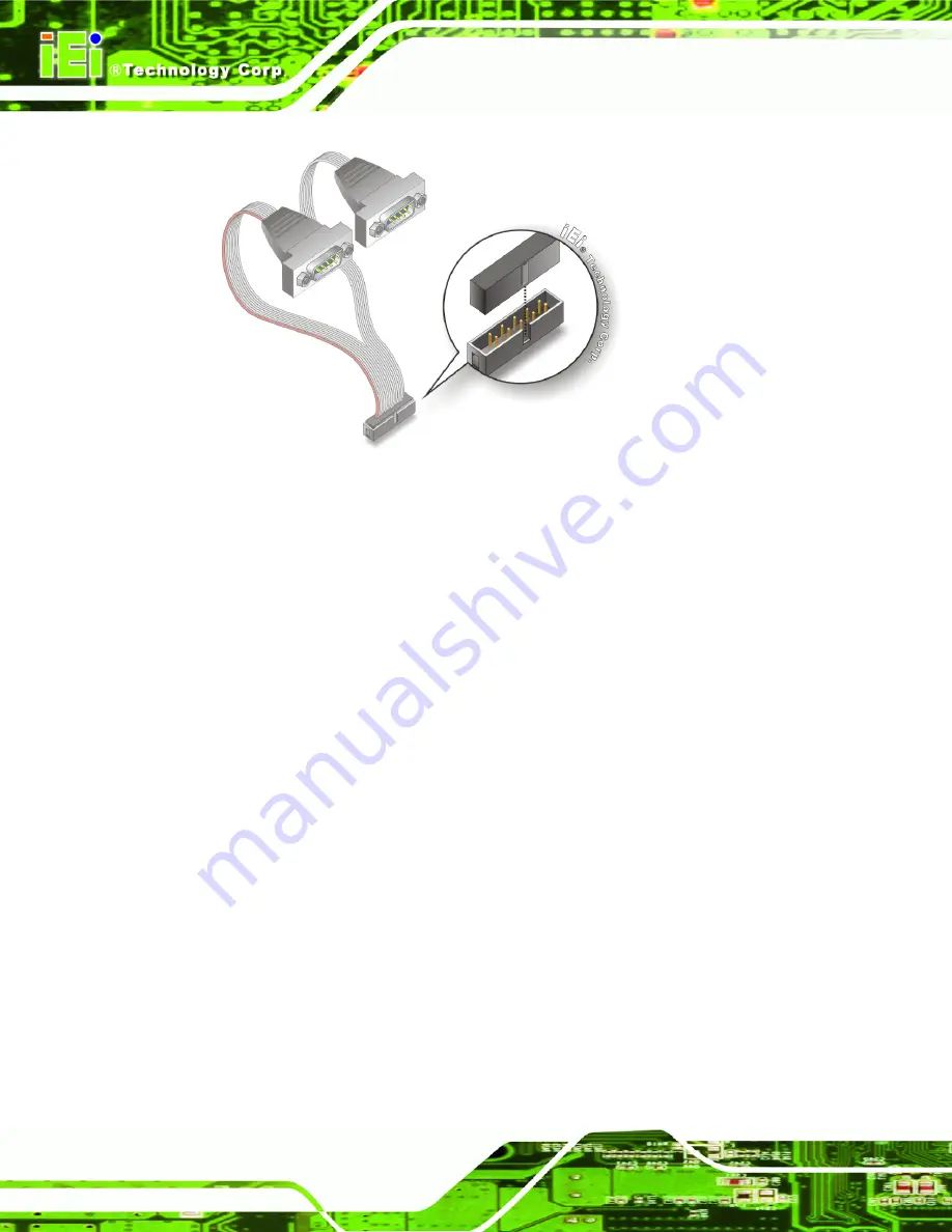
Figure 4-14: Dual RS-232 Cable Installation 

Step 3: 

Secure the connectors

. Both single RS-232 connectors have two retention 

screws that must be secured to a chassis or bracket. 

Step 4: 

Connect the serial device

. Once the single RS-232 connectors are connected 

to a chassis or bracket, a serial communications device can be connected to the 

system. 

Step 0:


4.8.4 Keyboard/Mouse Y-cable Connector 

The WAFER-945GSELVDS2 is shipped with a keyboard/mouse Y-cable connector. The 

keyboard/mouse Y-cable connector connects to a keyboard/mouse connector on the 

WAFER-945GSELVDS2 and branches into two cables that are each connected to a PS/2 

connector, one for a mouse and one for a keyboard. To connect the keyboard/mouse 

Y-cable connector please follow the steps below. 

Step 1: 

Locate the connector

. The location of the keyboard/mouse Y-cable connector 

is shown in 

Chapter 3

Step 2: 

Align the connectors

. Correctly align pin 1 on the cable connector with pin 1 on 

the WAFER-945GSELVDS2 keyboard/mouse connector. See 

Figure 4-15

Summary of Contents for WAFER-945GSELVDS2-N270-R10

Page 1: ...5GSELVDS2 Page i IEI Technology Corp User Manual MODEL WAFER 945GSELVDS2 3 5 SBC with 1 6 GHz Intel ATOM N270 VGA Dual LVDS Gigabit Ethernet CompactFlash Audio and SATA RoHS Compliant Rev 1 01 12 Augu...

Page 2: ...WAFER 945GSELVDS2 Page ii Revision Date Version Changes 12 August 2011 1 01 Modified SATA connector description 24 September 2009 1 00 Initial release...

Page 3: ...rising out of the use or inability to use the product or documentation even if advised of the possibility of such damages This document contains proprietary information protected by copyright All righ...

Page 4: ...nal Items 11 3 CONNECTORS 12 3 1 PERIPHERAL INTERFACE CONNECTORS 13 3 2 PERIPHERAL INTERFACE CONNECTORS 13 3 2 1 Internal Peripheral Connectors 13 3 2 2 External Interface Panel Connectors 14 3 3 INTE...

Page 5: ...37 3 4 2 Serial Port Connector 38 3 4 3 USB Connectors 38 3 4 4 VGA Connector 39 4 INSTALLATION 40 4 1 ANTI STATIC PRECAUTIONS 41 4 2 INSTALLATION CONSIDERATIONS 42 4 2 1 Installation Notices 42 4 2 2...

Page 6: ...onitor Connection 65 4 10 HEAT SINK ENCLOSURE 66 4 11 INSTALLING DRIVERS 67 5 BIOS 70 5 1 INTRODUCTION 71 5 1 1 Starting Setup 71 5 1 2 Using Setup 71 5 1 3 Getting Help 72 5 1 4 Unable to Reboot Afte...

Page 7: ...105 5 7 2 Southbridge Configuration 108 5 8 EXIT 109 A BIOS OPTIONS 111 B TERMINOLOGY 115 C DIGITAL I O INTERFACE 119 C 1 INTRODUCTION 120 C 2 DIO CONNECTOR PINOUTS 120 C 3 ASSEMBLY LANGUAGE SAMPLES 1...

Page 8: ...21 Figure 3 8 CPU Fan Connector Location 22 Figure 3 9 Keyboard Mouse Connector Location 23 Figure 3 10 LED Connector Locations 24 Figure 3 11 LVDS1 Location 25 Figure 3 12 Backlight Connector Pinout...

Page 9: ...ction Jumper Pinout Locations 54 Figure 4 10 LVDS Voltage Selection Jumper Pinout Locations 55 Figure 4 11 Audio Kit Cable Connection 57 Figure 4 12 SATA Drive Cable Connection 58 Figure 4 13 SATA Pow...

Page 10: ...able 3 10 Keyboard Mouse Connector Pinouts 23 Table 3 11 LED Connector Pinouts 24 Table 3 12 LVDS1 Pinouts 25 Table 3 13 Backlight Connector Pinouts 26 Table 3 14 LVDS2 Pinouts 28 Table 3 15 Backlight...

Page 11: ...F Card Setup Jumper Settings 49 Table 4 5 Clear CMOS Jumper Settings 51 Table 4 6 COM 2 Function Select Jumper Settings 51 Table 4 7 LVDS1 Panel Resolution 52 Table 4 8 LVDS2 Panel Resolution 52 Table...

Page 12: ...ion 88 BIOS Menu 11 Remote Access Configuration 90 BIOS Menu 12 USB Configuration 93 BIOS Menu 13 USB Mass Storage Device Configuration 95 BIOS Menu 14 PCI PnP Configuration 97 BIOS Menu 15 Boot 98 BI...

Page 13: ...WAFER 945GSELVDS2 Page 1 Chapter 1 1 Introduction...

Page 14: ...SELVDS2 has 18 bit and 24 bit dual channel LVDS connectors and a single VGA video output External connectors include USB and Gigabit Ethernet connectors Expansion options include SATA slots a PCIe Min...

Page 15: ...Technical Specifications WAFER 945GSELVDS2 technical specifications are listed in Table 1 1 See Chapter 2 for details Specification WAFER 945GSELVDS2 Form Factor 3 5 System CPU 1 6 GHz Intel ATOM N27...

Page 16: ...11CP PCIe GbE chips COM 3 x RS 232 serial ports one external two internal 1 x RS 232 422 485 serial port internal USB2 0 6 x USB four external two internal SATA Two 3 0 Gb s SATA drives supported Keyb...

Page 17: ...WAFER 945GSELVDS2 Page 5 1 4 Dimensions The dimensions of the board are shown below Figure 1 3 Main Dimensions mm...

Page 18: ...WAFER 945GSELVDS2 Page 6 Figure 1 4 Bottom Dimensions mm Figure 1 5 External Interface Panel Dimensions mm...

Page 19: ...7 1 5 Data Flow Figure 1 6 shows the data flow between the two on board chipsets and other components installed on the motherboard and described in the following sections of this chapter Figure 1 6 D...

Page 20: ...WAFER 945GSELVDS2 Page 8 Chapter 2 2 Unpacking...

Page 21: ...istband can help to prevent ESD from damaging the board Self grounding Before handling the board touch any grounded conducting material During the time the board is handled frequently touch any conduc...

Page 22: ...ased from or contact an IEI sales representative directly by sending an email to sales iei com tw 2 3 1 Package Contents The WAFER 945GSELVDS2 is shipped with the following components Quantity Item an...

Page 23: ...e 2 1 Packing List 2 3 2 Optional Items The WAFER 945GSELVDS2 is shipped with the following components Item and Part Number Image Dual USB cable wo bracket P N 32000 070301 RS RS 232 422 485 cable P N...

Page 24: ...WAFER 945GSELVDS2 Page 12 Chapter 3 3 Connectors...

Page 25: ...ace Connectors Table 3 1 shows a list of the peripheral interface connectors on the WAFER 945GSELVDS2 Detailed descriptions of these connectors can be found below 3 2 1 Internal Peripheral Connectors...

Page 26: ...Mini Card slot PCIe Mini Slot CN4 Power Button 2 pin wafer PWRBTN1 Reset button connector 2 pin header RESET1 Serial ATA SATA drive connectors 7 pin SATA SATA1 SATA2 Serial port 10 pin header COM3 CO...

Page 27: ...f all the internal peripheral connectors on the WAFER 945GSELVDS2 3 3 1 ATX Power Connector CN Label ATXPWR1 CN Type 4 pin AT power connector 1x4 CN Location See Figure 3 2 CN Pinouts See Table 3 3 Th...

Page 28: ...2 3 for AT power use or connect to power control cable for ATX power control use Figure 3 3 ATX Power Control Connector Location Pin Description 1 5V Standby 2 GND 3 PS_ON Table 3 4 ATX Power Supply...

Page 29: ...and from the system Figure 3 4 Audio Connector Pinouts Pin Description Pin Description 1 Line out R 2 Line in R 3 GND 4 GND 5 Line out L 6 Line in L 7 GND 8 GND 9 MIC in 10 Mic in Table 3 5 Audio Conn...

Page 30: ...The battery provides power to the system clock to retain the time when power is turned off Figure 3 5 Battery Connector Location Pin Description 1 Battery 2 Ground Table 3 6 Battery Connector Pinouts...

Page 31: ...Card Slot Location Pin Description Pin Description 1 GND 26 CD1 2 D3 27 D11 3 D4 28 D12 4 D5 29 D13 5 D6 30 D14 6 D7 31 D15 7 CE 32 CE2 8 A10 33 VS1 9 OE 34 IOR 10 A9 35 IOW 11 A8 36 WE 12 A7 37 IRQ 1...

Page 32: ...D0 46 BVD1 22 D1 47 D8 23 D2 48 D9 24 IOCS16 49 D10 25 CD2 50 GND2 Table 3 7 CF Card Slot Pinouts 3 3 6 Digital I O Connector CN Label DIO1 CN Type 10 pin header 2x5 CN Location See Figure 3 7 CN Pino...

Page 33: ...Description 1 GND 2 VCC 3 Output 3 4 Output 2 5 Output 1 6 Output 0 7 Input 3 8 Input 2 9 Input 1 10 Input 0 Table 3 8 Digital I O Connector Location 3 3 7 CPU Fan Connector CN Label CPU_FAN1 CN Type...

Page 34: ...ct Table 3 9 CPU Fan Connector Pinouts 3 3 8 Keyboard Mouse Connector CN Label KB_MS1 CN Type 6 pin header 1x6 CN Location See Figure 3 9 CN Pinouts See Table 3 10 The keyboard and mouse connector can...

Page 35: ...6 GROUND Table 3 10 Keyboard Mouse Connector Pinouts 3 3 9 LED Connector CN Label LED_C1 CN Type 6 pin wafer 1x6 CN Location See Figure 3 10 CN Pinouts See Table 3 11 The LED connector connects to an...

Page 36: ...D 3 Power LED 4 Power LED 5 HDD LED 6 HDD LED Table 3 11 LED Connector Pinouts 3 3 10 LVDS1 LCD Connector CN Label LVDS1 CN Type 30 pin crimp 2x15 CN Location See Figure 3 11 CN Pinouts See Table 3 12...

Page 37: ...Description 1 GND1 2 GND2 3 A_Y0 4 A_Y0 5 A_Y1 6 A_Y1 7 A_Y2 8 A_Y2 9 A_CK 10 A_CK 11 NC 12 NC 13 GND3 14 GND4 15 B_Y0 16 B_Y0 17 B_Y1 18 B_Y1 19 B_Y2 20 B_Y2 21 B_CK 22 B_CK 23 NC 24 NC 25 GND5 26 G...

Page 38: ...CN Pinouts See Table 3 13 Provides power to an LVDS monitor Figure 3 12 Backlight Connector Pinout Locations Pin Description 1 LCD Backlight Control 2 GROUND 3 12V 4 GROUND 5 BACKLIGHT Enable Table 3...

Page 39: ...any compatible LVDS monitor Figure 3 13 LVDS2 Location Pin Description Pin Description 1 GND1 2 GND2 3 A_Y0 4 A_Y0 5 A_Y1 6 A_Y1 7 A_Y2 8 A_Y2 9 A_CK 10 A_CK 11 A_Y3 12 A_Y3 13 GND3 14 GND4 15 B_Y0 1...

Page 40: ...LVDS2 Pinouts 3 3 13 LVDS2 Inverter Connector CN Label INVERTER2 CN Type 5 pin wafer 1x5 CN Location See Figure 3 12 CN Pinouts See Table 3 13 Provides power to an LVDS monitor Figure 3 14 Backlight...

Page 41: ...pin Mini PCIe Card Slot CN Location See Figure 3 15 CN Pinouts See Table 3 16 The PCIe mini card slot enables a PCIe mini card expansion module to be connected to the board Cards supported include amo...

Page 42: ...ual 25 PERP2 26 GND 27 GND 28 1 5V 29 GND 30 SMBCLK 31 PETN2 32 SMBDATA 33 PETP2 34 GND 35 GND 36 USBD 37 N C 38 USBD 39 N C 40 GND 41 N C 42 N C 43 N C 44 RF_LINK 45 N C 46 BLUELED 47 N C 48 1 5V 49...

Page 43: ...igure 3 16 Power Button Connector Location Pin Description 1 Power Switch 2 GND Table 3 17 Power Button Connector Pinouts 3 3 16 Reset Button Connector CN Label RESET1 CN Type 2 pin wafer 1x2 CN Locat...

Page 44: ...itch 2 GND Table 3 18 Reset Button Connector Pinouts 3 3 17 SATA Drive Connectors CN Label SATA1 SATA2 CN Type 7 pin SATA drive connectors CN Location See Figure 3 18 CN Pinouts See Table 3 19 The SAT...

Page 45: ...ons Pin Description 1 GND 2 TX 3 TX 4 GND 5 RX 6 RX 7 GND Table 3 19 SATA Drive Connector Pinouts 3 3 18 Serial Port Connector CN Label COM3 COM4 CN Type 10 pin header CN Location See Figure 3 19 CN P...

Page 46: ...ector RS 232 422 485 CN Label COM2 CN Type 14 pin header 2x7 CN Location See Figure 3 20 CN Pinouts See Table 3 21 The 14 pin serial port connector connects to the COM2 serial communications channels...

Page 47: ...iption Pin Description 1 DCD 2 DSR 3 RXD 4 RTS 5 TXD 6 CTS 7 DTR 8 RI 9 GND 10 N C 11 TXD485 12 TXD485 13 RXD485 14 RXD485 Table 3 21 RS 232 RS 485 Serial Port Connector Pinouts 3 3 20 USB Connector C...

Page 48: ...ternal USB ports are found on the rear panel The USB ports are used for I O bus expansion Figure 3 21 USB Connector Pinout Locations Pin Description Pin Description 1 VCC 2 GND 3 DATA 4 DATA 5 DATA 6...

Page 49: ...ting the status of LAN The pin assignments are listed in the following table Pin Description Pin Description 1 MDIA3 5 MDIA1 2 MDIA3 6 MDIA2 3 MDIA2 7 MDIA0 4 MDIA1 8 MDIA0 Table 3 23 LAN Pinouts Figu...

Page 50: ...to RS 232 serial communications devices Pin Description Pin Description 1 DCD 6 DSR 2 RX 7 RTS 3 TX 8 CTS 4 DTR 9 RI 5 GND Table 3 25 Serial Port Pinouts Figure 3 24 Serial Port Pin Location 3 4 3 US...

Page 51: ...5 pin Female CN Location See Figure 3 22 CN Pinouts See Figure 3 25 and Table 3 27 The WAFER 945GSELVDS2 has a single 15 pin female connector for connectivity to standard display devices Figure 3 25 V...

Page 52: ...WAFER 945GSELVDS2 Page 40 Chapter 4 4 Installation...

Page 53: ...y other electrical component is handled the following anti static precautions are strictly adhered to Wear an anti static wristband Wearing a simple anti static wristband can help to prevent ESD from...

Page 54: ...ructions described in this manual should be carefully followed in order to prevent damage to the WAFER 945GSELVDS2 WAFER 945GSELVDS2 components and injury to the user Before and during the installatio...

Page 55: ...connector pins or its components 4 2 2 Installation Checklist The following checklist is provided to ensure the WAFER 945GSELVDS2 is properly installed All the items in the packing list are present A...

Page 56: ...y damage the WAFER 945GSELVDS2 Please make sure the purchased SO DIMM complies with the memory specifications of the WAFER 945GSELVDS2 SO DIMM specifications compliant with the WAFER 945GSELVDS2 are l...

Page 57: ...945GSELVDS2 can support both CF Type I cards and CF Type II cards For the complete specifications of the supported CF cards please refer to Chapter 2 To install the a CF card Type 1 or Type 2 onto the...

Page 58: ...lose an electrical circuit It consists of two or three metal pins and a small metal clip often protected by a plastic cover that slides over the pins to connect them To CLOSE SHORT a jumper means conn...

Page 59: ...in header COM2 Mode Setting JP1 6 pin header LVDS1 Panel Resolution J_LCD_TYPE1 8 pin header LVDS1 voltage selection J_VLVDS1 3 pin header LVDS2 voltage selection J_VLVDS2 3 pin header Table 4 1 Jumpe...

Page 60: ...udio Power Source Jumper Label JP2 Jumper Type 3 pin header Jumper Settings See Table 4 3 Jumper Location See Figure 4 4 Sets the power source for the onboard audio The 12 V power converted to 5 V thr...

Page 61: ...pin header Jumper Settings See Table 4 4 Jumper Location See Figure 4 5 The CF Card Setup jumper sets the CF Type I card or CF Type II cards as either the slave device or the master device CF Card Set...

Page 62: ...tem BIOS information To do this use the jumper cap to close pins 2 and 3 for a few seconds then reinstall the jumper clip back to pins 1 and 2 If the CMOS Settings Wrong message is displayed during th...

Page 63: ...8 pin header Jumper Settings See Table 4 6 Jumper Location See Figure 4 7 The COM 2 Function Select jumper sets the communication protocol used by the second serial communications port COM 2 as RS 23...

Page 64: ...e 4 8 Sets the resolution of both LVDS1 and LVDS2 video channels Pin LVDS1 Resolution Open 800 x 600 18 bit 1 2 1024 x 768 18 bit 3 4 1280 x 1024 36 bit 1 2 3 4 1400 x 1050 36 bit Table 4 7 LVDS1 Pane...

Page 65: ...f the wrong voltage is selected with this jumper Please refer to the user guide that came with the monitor to select the correct voltage Jumper Label J_VLVDS1 Jumper Type 3 pin header Jumper Settings...

Page 66: ...wrong voltage is selected with this jumper Please refer to the user guide that cam with the monitor to select the correct voltage Jumper Label J_VLVDS2 Jumper Type 3 pin header Jumper Settings See Tab...

Page 67: ...The WAFER 945GSELVDS2 must be installed in a chassis with ventilation holes on the sides allowing airflow to travel through the heat sink surface In a system with an individual power supply unit the c...

Page 68: ...audio connector on the WAFER 945GSELVDS2 The audio kit consists of three audio jacks Mic in connects to a microphone Line in provides a stereo line level input to connect to the output of an audio dev...

Page 69: ...evice to the line in audio jack Connect a microphone to the mic in audio jack Step 0 4 8 2 SATA Drive Connection The WAFER 945GSELVDS2 is shipped with two SATA drive cables and one SATA drive power ca...

Page 70: ...ble Connection Step 3 Connect the cable to the SATA disk Connect the connector on the other end of the cable to the connector at the back of the SATA drive See Figure 4 13 NOTE The SATA power cable de...

Page 71: ...ached to a D sub 9 pin male connector To install the dual RS 232 cable please follow the steps below Step 1 Locate the connectors The locations of the RS 232 connectors are shown in Chapter 3 Step 2 I...

Page 72: ...e WAFER 945GSELVDS2 is shipped with a keyboard mouse Y cable connector The keyboard mouse Y cable connector connects to a keyboard mouse connector on the WAFER 945GSELVDS2 and branches into two cables...

Page 73: ...assis The keyboard mouse Y cable connector is connected to two PS 2 connectors To secure the PS 2 connectors to the chassis please refer to the installation instructions that came with the chassis Ste...

Page 74: ...two connectors Correctly align pin 1on each cable connector with pin 1 on the WAFER 945GSELVDS2 USB connector Step 3 Insert the cable connectors Once the cable connectors are properly aligned with th...

Page 75: ...network To connect a LAN cable with an RJ 45 connector please follow the instructions below Step 1 Locate the RJ 45 connectors The locations of the USB connectors are shown in Chapter 4 Step 2 Align...

Page 76: ...he serial connector Insert the DB 9 connector of a serial device into the DB 9 connector on the external peripheral interface See Figure 4 18 Figure 4 18 Serial Device Connector Step 3 Secure the conn...

Page 77: ...Connector 4 9 4 VGA Monitor Connection The WAFER 945GSELVDS2 has a single female DB 15 connector on the external peripheral interface panel The DB 15 connector is connected to a CRT or VGA monitor To...

Page 78: ...igure 4 20 VGA Connector Step 4 Secure the connector Secure the DB 15 VGA connector from the VGA monitor to the external interface by tightening the two retention screws on either side of the connecto...

Page 79: ...ER 945GSELVDS2 on a heat dissipation surface or using copper pillars to hold the board up from the desk below When the WAFER 945GSELVDS2 is shipped it is secured to a heat sink with five retention scr...

Page 80: ...WAFER 945GSELVDS2 Page 68 Step 1 Insert the CD ROM that came with the system into a CD ROM drive attached to the system Step 2 The screen in Figure 4 22 appears Figure 4 22 Start Up Screen...

Page 81: ...WAFER 945GSELVDS2 Page 69 Step 3 Select the operating system Figure 4 23 Select Operating System Step 4 Install all the drivers from the list S t e p 0 Figure 4 24 Drivers...

Page 82: ...WAFER 945GSELVDS2 Page 70 Chapter 5 5 BIOS...

Page 83: ...restart the computer and try again 5 1 2 Using Setup Use the arrow keys to highlight items press ENTER to select use the PageUp and PageDown keys to change entries press F1 for help and press ESC to...

Page 84: ...t after BIOS changes are made the BIOS will either automatically reset to default settings or can be manually reset using the Clear CMOS jumper 5 1 5 BIOS Menu Bar The menu bar on top of the BIOS scre...

Page 85: ...t Item Enter Go to SubScreen F1 General Help F10 Save and Exit ESC Exit v02 61 Copyright 1985 2006 American Megatrends Inc BIOS Menu 1 Main System Overview The System Overview lists a brief summary of...

Page 86: ...re the CPU and peripheral devices through the following sub menus BIOS SETUP UTILITY Main Advanced PCIPNP Boot Security Chipset Exit Advanced Settings WARNING Setting wrong values in below sections ma...

Page 87: ...Ratio Actual Value 12 Select Screen Select Item Enter Go to SubScreen F1 General Help F10 Save and Exit ESC Exit v02 61 Copyright 1985 2006 American Megatrends Inc BIOS Menu 3 CPU Configuration The CP...

Page 88: ...nter Go to SubScreen F1 General Help F10 Save and Exit ESC Exit v02 61 Copyright 1985 2006 American Megatrends Inc BIOS Menu 4 IDE Configuration ATA IDE Configurations Compatible Use the ATA IDE Confi...

Page 89: ...are shown in the IDE Configuration menu Primary IDE Master Primary IDE Slave 5 3 2 1 IDE Master IDE Slave Use the IDE Master and IDE Slave configuration menu to view both primary and secondary IDE dev...

Page 90: ...be transferred per interrupt if block mode is not used Block mode allows transfers of up to 64 KB per interrupt PIO Mode Indicates the PIO mode of the installed device Async DMA Indicates the highest...

Page 91: ...e In LBA mode the maximum drive capacity is 137 GB Disabled BIOS is prevented from using the LBA mode control on the specified channel Auto DEFAULT BIOS auto detects the LBA mode control on the specif...

Page 92: ...a maximum transfer rate of 16 6 MB s This setting generally works with all hard disk drives manufactured after 1999 For other disk drives such as IDE CD ROM drives check the specifications of the driv...

Page 93: ...e S M A R T option to auto detect disable or enable Self Monitoring Analysis and Reporting Technology SMART on the drive on the specified channel S M A R T predicts impending drive failures The S M A...

Page 94: ...RQ3 Serial Port3 Address 3E8 Serial Port3 IRQ 11 Serial Port4 Address 2E8 Serial Port4 IRQ 10 Allows BIOS to select Serial Port Base Addresses Select Screen Select Item Enter Go to SubScreen F1 Genera...

Page 95: ...ss of serial port Disabled 3E8 DEFAULT 2E8 2F0 2E0 Serial Port3 IRQ 11 Sets the IRQ of serial port 10 11 DEFAULT Serial Port4 Address 3F8 Sets the address of serial port Disabled 3E8 2E8 DEFAULT 2F0 2...

Page 96: ...184 V 1 05V 1 024 V 3 30V 3 296 V 5 00V 4 919 V 12 0V 12 480 V 1 5V 1 488 V 1 8V 1 792 V 5VSB 4 919 V VBAT 3 296 V Select Screen Select Item F1 General Help F10 Save and Exit ESC Exit v02 61 Copyright...

Page 97: ...27 C CPU Temperature Limit of Start 020 WARNING CPU failure can result if this value is set too high because permanent damage will be done before it turns on The fan will start spinning when this temp...

Page 98: ...ipset Power Exit Power Configuration Select AT ATX Power BY HARDWARE Current Jumper Setting AT Power If set to BY HARDWARE the status is set by the onboard jumper Select Screen Select Item Enter Go to...

Page 99: ...ate to use for system suspend Select Screen Select Item Enter Go to SubScreen F1 General Help F10 Save and Exit ESC Exit v02 61 Copyright 1985 2006 American Megatrends Inc BIOS Menu 9 ACPI Configurati...

Page 100: ...elect Screen Select Item Enter Go to SubScreen F1 General Help F10 Save and Exit ESC Exit v02 61 Copyright 1985 2006 American Megatrends Inc BIOS Menu 10 APM Configuration Restore on AC Power Loss Las...

Page 101: ...ivity on the keyboard or mouse Resume on Ring Disabled Use the Resume on Ring BIOS option to enable activity on the RI ring in modem line to rouse the system from a suspend or standby state That is th...

Page 102: ...the Remote Access Configuration menu to configure remote access parameters The Remote Access Configuration is an AMIBIOS feature and allows a remote host running a terminal program to display and con...

Page 103: ...se configuration options are discussed below Serial Port Number COM1 Use the Serial Port Number option allows to select the serial port used for remote access COM1 DEFAULT COM2 COM3 COM4 COM5 COM6 Bas...

Page 104: ...n to specify when console redirection should occur Disabled The console is not redirected after POST Boot Loader Redirection is active during POST and during Boot Loader Always DEFAULT Redirection is...

Page 105: ...Disabled Enabled Select Screen Select Item Enter Go to SubScreen F1 General Help F10 Save and Exit ESC Exit v02 61 Copyright 1985 2006 American Megatrends Inc BIOS Menu 12 USB Configuration USB Functi...

Page 106: ...en this option is enabled any attached USB mouse or USB keyboard can control the system even when there is no USB driver loaded onto the system Disabled Legacy USB support disabled Enabled DEFAULT Leg...

Page 107: ...rican Megatrends Inc BIOS Menu 13 USB Mass Storage Device Configuration USB Mass Storage Reset Delay 20 Sec Use the USB Mass Storage Reset Delay option to set the number of seconds POST waits for the...

Page 108: ...responding to INT13h calls that return DL 0 or DL 1 respectively Forced FDD Allows a hard disk image to be connected as a floppy image This option works only for drives formatted with FAT12 FAT16 or...

Page 109: ...lable DMA Channel 3 Available DMA Channel 5 Available DMA Channel 6 Available DMA Channel 7 Available Available Specified IRQ is available to be used by PCI PnP devices Reserved Specified IRQ is reser...

Page 110: ...for legacy ISA devices 64K 64 KB reserved for legacy ISA devices 5 5 Boot Use the Boot menu to configure system boot options BIOS SETUP UTILITY Main Advanced PCIPNP Boot Security Chipset Exit Boot Se...

Page 111: ...to boot the system Select Screen Select Item Enter Go to SubScreen F1 General Help F10 Save and Exit ESC Exit v02 61 Copyright 1985 2006 American Megatrends Inc BIOS Menu 16 Boot Settings Configurati...

Page 112: ...e the keyboard Number Lock automatically To use the 10 keys on the keyboard press the Number Lock key located on the upper left hand corner of the 10 key pad The Number Lock LED on the keyboard lights...

Page 113: ...on BIOS SETUP UTILITY Main Advanced PCIPNP Boot Security Chipset Exit Boot Device Priority 1st Boot Device 1st Boot Device 2nd Boot Device 2nd Boot Device 3rd Boot Device 3rd Boot Device Specifies the...

Page 114: ...e and Exit ESC Exit v02 61 Copyright 1985 2006 American Megatrends Inc BIOS Menu 18 Hard Disk Drives 5 5 4 Removable Drives Use the Removable Drives menu BIOS Menu 19 to specify the boot sequence of t...

Page 115: ...ect Item Enter Go to SubScreen F1 General Help F10 Save and Exit ESC Exit v02 61 Copyright 1985 2006 American Megatrends Inc BIOS Menu 20 CD DVD Drives 5 6 Security Use the Security menu to set system...

Page 116: ...s Not Installed If a user password must be installed select this field and enter the password After the password has been added Install appears next to Change User Password 5 7 Chipset Use the Chipset...

Page 117: ...nter Go to SubScreen F1 General Help F10 Save and Exit ESC Exit v02 61 Copyright 1985 2006 American Megatrends Inc BIOS Menu 23 Northbridge Chipset Configuration Memory Hole Disabled Use the Memory Ho...

Page 118: ...memory DVMT Mode DEFAULT Graphics memory is dynamically allocated according to the system and graphics needs Combo Mode A fixed portion of graphics memory is reserved as graphics memory If more memor...

Page 119: ...by H W Selects the screen resolution of LVDS1 640x480 18 bit 800x480 18 bit 800x600 18 bit 1024x768 18 bit 1280x1024 36 bit 1400x1050 36 bit 1440x900 36 bit 1600x1200 36 bit by H W DEFAULT LVDS1 Curr...

Page 120: ...merican Megatrends Inc BIOS Menu 24 Southbridge Chipset Configuration Audio Controller Codec Auto This option enables and disables the audio controller When disabled there will be no sound from the sy...

Page 121: ...0 key can be used for this operation Select Screen Select Item Enter Go to SubScreen F1 General Help F10 Save and Exit ESC Exit v02 61 Copyright 1985 2006 American Megatrends Inc BIOS Menu 25 Exit Sav...

Page 122: ...ad the optimal default values for each of the parameters on the Setup menus F9 key can be used for this operation Load Failsafe Defaults Use the Load Failsafe Defaults option to load failsafe default...

Page 123: ...WAFER 945GSELVDS2 Page 111 Appendix A A BIOS Options...

Page 124: ...A R T Auto 81 32Bit Data Transfer Enabled 81 Serial Port1 Address 3F8 IRQ4 82 Serial Port2 Address 2F8 IRQ3 82 Serial Port3 Address 3E8 83 Serial Port3 IRQ 11 83 Serial Port4 Address 3F8 83 Serial Por...

Page 125: ...Available 97 Reserved Memory Size Disabled 98 Quick Boot Enabled 99 Quiet Boot Disabled 99 AddOn ROM Display Mode Force BIOS 100 Bootup Num Lock On 100 Boot From LAN Support Disabled 100 Change Super...

Page 126: ...WAFER 945GSELVDS2 Page 114 Save Changes and Exit 109 Discard Changes and Exit 109 Discard Changes 109 Load Optimal Defaults 110 Load Failsafe Defaults 110...

Page 127: ...WAFER 945GSELVDS2 Page 115 Appendix B B Terminology...

Page 128: ...binary 0 while a high amplitude signal represents a binary 1 BIOS The Basic Input Output System BIOS is firmware that is first run when the computer is turned on and can be configured by the end user...

Page 129: ...ep Technology EIST allows users to modify the power consumption levels and processor performance through application software The application software changes the bus to core frequency ratio and the p...

Page 130: ...sfers between storage devices and the computer chipsets The SATA bus has transfer speeds up to 1 5 Gbps and the SATA II bus has data transfer speeds of up to 3 0 Gbps S M A R T Self Monitoring Analysi...

Page 131: ...WAFER 945GSELVDS2 Page 119 Appendix C C Digital I O Interface...

Page 132: ...sheet for the Super I O chipset C 2 DIO Connector Pinouts The following table describes how the DIO connector pins are connected to the Super I O GPIO port 1 Pin Description Super I O Pin Super I O Pi...

Page 133: ...l I O input functions is listed below MOV AX 6F08H Sets the digital port as input INT 15H Initiates the INT 15H BIOS call C 3 2 Enable the DIO Output Function The BIOS interrupt call INT 15H controls...

Page 134: ...WAFER 945GSELVDS2 Page 122 Appendix D D Watchdog Timer...

Page 135: ...S function call INT 15H is used to control the Watchdog Timer INT 15H AH 6FH Sub function AL 2 Sets the Watchdog Timer s period BL Time out value Its unit second is dependent on the item Watchdog Time...

Page 136: ...stem resets EXAMPLE PROGRAM INITIAL TIMER PERIOD COUNTER W_LOOP MOV AX 6F02H setting the time out value MOV BL 30 time out value is 48 seconds INT 15H ADD THE APPLICATION PROGRAM HERE CMP EXIT_AP 1 is...

Page 137: ...WAFER 945GSELVDS2 Page 125 Appendix E E Hazardous Materials Disclosure...

Page 138: ...esences of small quantities of certain materials in the product and is applicable to China RoHS only A label will be placed on each product to indicate the estimated Environmentally Friendly Use Perio...

Page 139: ...Board X O O O O X Metal Fasteners X O O O O O Cable Assembly X O O O O X Fan Assembly X O O O O X Power Supply Assemblies X O O O O X Battery O O O O O O O This toxic or hazardous substance is contain...

Page 140: ...WAFER 945GSELVDS2 Page 128 RoHS RoHS Pb Hg Cd CR VI PBB PBDE X O O O O X X O O O O X X O O O O X X O O O O O X O O O O X X O O O O X X O O O O X O O O O O O O SJ T11363 2006 X SJ T11363 2006...

Reviews: