background image


4.  Demo Programs 

4.  Demo Programs 


4.1  Demo Programs for Windows 

4.1  Demo Programs for Windows 


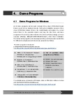
All of demo programs will not work normally if DLL driver (PISO-DA2 Classic 
Driver) would not be installed correctly. During the installation process of DLL 
driver (PISO-DA2 Classic Driver), the install-shields will register the correct 
kernel driver to the operation system and copy the DLL driver and demo 
programs to the correct position based on the driver software package you have 
selected (Windows 98/Me/NT/2000/XP/2003/Vista/7). After driver installation, 
the related demo programs and development library and declaration header files 
for different development environments are presented as follows.  


The demo program is


located at: 

CD:\NAPDOS\PCI\PISO-DA2\DLL\Demo\ 

http://ftp.icpdas.com/pub/cd/iocard/pci/napdos/pci/piso-da2/dll/demo/ 


„


BCB 3  

Æ

 For Borland C

++ 

Builder 3 

PISODA.H 

Æ

 Header files 


„


DEMO4: Two cards D/A output

„


DEMO3: Read/Write from/to 

EEPROM and software 
calibration. 

„


DEMO2: D/A output 


„


DEMO1: Get cards information

A list of available demo 
programs is as follows: 


PISODA.LIB 

Æ

 Linkage library for BCB


„


Delphi5  

Æ

 For Delphi 5 


PISODA.PAS 

Æ

 Declaration files 


„


VB6  

Æ

 For Visual Basic 6 


PISODA.BAS 

Æ

 Declaration files 


„


VB.NET2005  

Æ

 For VB.NET2005 

PISODA.vb 

Æ

 Declaration files 

„

CSharp2005  

Æ

 For C#.NET2005 


PISODA.cs 

Æ

 Declaration files 

ODA.cs 

Æ

 Declaration files 


The detailed demo information of Windows refers to PISO-DA2 software manual 
(CD:\NAPDOS\PCI\PISO-DA2\Manual\). 

http://ftp.icpdas.com/pub/cd/iocard/pci/napdos/pci/piso-da2/manual/ 


PISO-DA2/DA2U User Manual (Ver.2.7, Mar. 2012, PMH-020-27)   


26


Summary of Contents for PISO-DA2

Page 1: ...the right to change this manual at any time without notice The information furnished by ICP DAS is believed to be accurate and reliable However no responsibility is assumed by ICP DAS for its use nor...

Page 2: ...NNECTION 18 2 5 1 Voltage Output Connection 18 2 5 2 Current Sink Connection 19 2 5 3 Current sink with internal power supply 19 2 6 OUTPUT RANGE AND RESOLUTION 20 2 7 CALIBRATION 21 3 SOFTWARE INSTAL...

Page 3: ...2 5 2 4 INT Mask Control Register 33 5 2 5 Aux Status Register 33 5 2 6 Interrupt Polarity Control Register 34 5 2 7 D A Data Output 34 5 2 8 Jumper Status Register 35 5 2 9 Read Card ID Register 36 P...

Page 4: ...20 mA and 4 20 mA In addition the PISO DA2U also features the following advantages by ICP DAS s innovation 1 Accurate and easy to use calibration ICP DAS provides the software calibration instead of...

Page 5: ...0 V 5 V Unipolar 0 10 V 0 5 V Current output Current loop sink 0 20 mA 4 20 mA Software calibration Unipolar or bipolar output available from each converter Two pacer timer interrupt source Double buf...

Page 6: ...niversal PCI 32 bit 33 MHz Data Bus 8 bit Card ID No Yes 4 bit I O Connector Female DB9 x 2 Dimensions L x W x D 170mm x 122mm x 22mm 189mm x 98mm x 22mm Power Consumption 1350 mA 5 V Operating Temper...

Page 7: ...6R16 P16C16 P16POR16 P8R8 D I O family isolated PCI TMC12 timer counter card non isolated PIO series cost effective non isolated cards PIO 823 821 multi function family PIO D168 D144 D96 D64 D56 D48 D...

Page 8: ...ion is given in the Quick Start Guide including Where to get the software driver demo programs and other resources How to install the software How to test the card Attention If any of these items are...

Page 9: ...ut PISO DA2 s Layout PCI BUS 4 20mA INT EXT 4 20mA 5V 10V EXT JP7 JP10 JP8 10V 5V JP3 JP6 JP4 JP5 BP UP JP9 BP UP JP1 JP2 BP BP UP UP PCI controller PISO DA2 CN2 CN1 INT CN1 The terminal of D A conver...

Page 10: ...converter channel 2 for voltage or current output JP1 JP2 JP5 JP9 Bipolar or Unipolar setting JP4 JP8 5 V or 10 V internal reference voltage setting JP3 JP7 0 20 mA or 4 20 mA current loop setting JP...

Page 11: ...t can be configured by jumper JP3 and JP7 for channel 1 and 2 respectively Note that each output channel can be set up as voltage or current output independently by using the corresponding setting jum...

Page 12: ...m the connector CN1 and CN2 The setting of the reference sources for Channel 1 and Channel 2 are controlled by the jumper JP6 and JP10 respectively as depicted in the following table2 3 Table 2 3 Sett...

Page 13: ...or 10 V which is precision voltage source provided by PISO DA2 DA2U by jumper JP4 Channel 1 and JP8 Channel 2 The detail setting method is illustrated as Table 2 4 The default setting is 5 V Table 2...

Page 14: ...jumper JP5 and JP9 The detail setting is demonstrated in Table 2 5 For example if the jumper JP4 and JP5 are set as 5 V and Unipolar respectively then the range of voltage output is 0 5 V for channel...

Page 15: ...s the output voltage by the setting of unipolar and internal reference voltage 5 V for each output channel in advance Then Jumper JP3 and JP7 of PSIO DA2 DA2U board can be utilized to select the curre...

Page 16: ...3 4 ID 0 ID 1 ID 2 ID 3 SW1 Default Settings Table 2 7 Default Settings OFF 1 ON 0 Card ID Hex 1 ID0 2 ID1 3 ID2 4 ID3 0x0 ON ON ON ON 0x1 OFF ON ON ON 0x2 ON OFF ON ON 0x3 OFF OFF ON ON 0x4 ON ON OF...

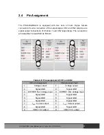
Page 17: ...s specified as follows Table 2 8 Pin assignment of CH1 and CH2 CN1 pin assignment CN2 pin assignment 1 Voltage output 1 Voltage output 2 Signal GND 2 Signal GND 3 EXTREF Ref Voltage Input 3 EXTREF Ref...

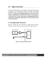
Page 18: ...lication the minimum load resistor must be bigger than 1 k However when current output function of PISO DA2 DA2U board is selected then the maximum load resistor of the current loop sink has to be sma...

Page 19: ...n external power is used 2 5 3 Current sink with internal power supply If your system does not offer external power supply a built in 15 VDC power source provided by PISO DA2 DA2U can be applied to bu...

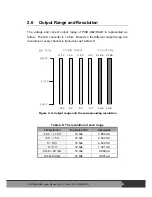
Page 20: ...ured out as Table 2 9 0x0FFF 0x000 0x7FF 10V 10V 5V 5V 10V 0V 0V 5V 20mA 20mA 0mA 4mA Hex Value Voltage Output Current Sink Figure 2 4 Output range and the corresponding revolution Table 2 9 The resol...

Page 21: ...dress in the first 16 words of the EEPROM as shown in Table 2 10 Table 2 10 Calibration values stored to the EEPROM address Output range The address of the EEPROM for CH1 The address of the EEPROM for...

Page 22: ...til the value is equal to the allowance maximum voltage output value Step 6 If the analog output is equal to the maximum allowance analog output it means that the calibration process is finished for t...

Page 23: ...E file in the NAPDOS folder on this CD Step 2 Click the item PCI Bus DAQ Card Step 3 Click the item UniDAQ Step 4 Click the item DLL for Windows 2000 and XP 2003 Vista 32 bit Step 5 Double Click UniDA...

Page 24: ...iocard pci napdos pci unidaq maunal Windows NT 2K and 32 bit Windows XP 2003 Vista 7 The PISODA DLL file will be copied into the Windows NT 2000 C WINNT SYSTEM32 folder Windows XP 2003 Vista 7 C WINDO...

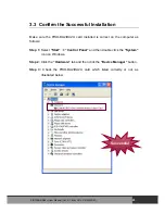
Page 25: ...llows Step 1 Select Start Control Panel and then double click the System icon on Windows Step 2 Click the Hardware tab and then click the Device Manager button Step 3 Check the PISO DA2 DA2U card whic...

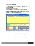
Page 26: ...ented as follows The demo program is located at CD NAPDOS PCI PISO DA2 DLL Demo http ftp icpdas com pub cd iocard pci napdos pci piso da2 dll demo BCB 3 For Borland C Builder 3 PISODA H Header files D...

Page 27: ...IB TC large model library file TC LIB Huge PIO H TC declaration file TC LIB Huge TCPIO_H LIB TC huge model library file MSC LIB Large PIO H MSC declaration file MSC LIB Large MSCPIO_L LIB MSC large mo...

Page 28: ...stage The fixed IDs for the PIO PISO series cards are shown in the tables below PISO DA2 PISO DA2 PISO DA2U Tiger 100 Tiger 320 Vendor ID 0xE159 0xE159 0xE159 Device ID 0x0002 0x0001 0x0001 Sub vendo...

Page 29: ...are installed in the PC will be shown as illustrated below Figure 5 1 PIO_PISO EXE Note The PIO_PISO EXE application is valid for all PIO PISO cards The user can execute the PIO_PISO EXE file to retr...

Page 30: ...D I O 80 01 40 PIO 823 Multi function 80 03 00 PIO 821 Multi function 80 03 10 PIO DA16 16 D A 80 04 00 PIO DA8 8 D A 80 04 00 PIO DA4 4 D A 80 04 00 PISO C64 64 isolated D O 80 08 00 PISO P64 64 iso...

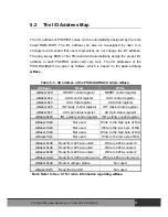
Page 31: ...AUX data register AUX data register wBase 0x5 INT mask control register INT mask control register wBase 0x7 AUX pin status register AUX pin status register wBase 0x2a INT polarity control register IN...

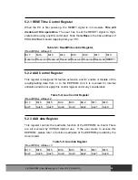
Page 32: ...r disable of the reading writing data from or to the EEPROM And it is reversed for internal utilization and do not apply this control register under any consideration Table 5 4 Aux Control Register Re...

Page 33: ...e information please refer to the DOS demo program demo1 c outportb wBase 5 0 disable all interrupts outportb wBase 5 1 enable interrupt of INT0 outportb wBase 5 2 enable interrupt of INT1 outportb wB...

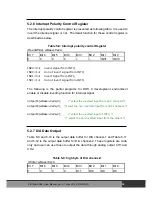
Page 34: ...pment environment enable or disable inverting function for interrupt signal outportb wBase 0x2a 0 select the inverted input from all 2 channels outportb wBase 0x2a 3 select the non inverted input from...

Page 35: ...Bit 1 Bit 0 X x JP9 JP8 JP7 JP5 JP4 JP3 JP3 0 JP3 is set at 0 20 mA for the current output of channel 1 JP3 1 JP3 is set at 4 20 mA for the current output of channel 1 JP4 0 JP4 is set at 10 V for int...

Page 36: ...ther their program is accessing the correct card About the detail information for Card ID register please refer to the following description Table 5 14 Read Card ID register Read wBase 0xf0 Bit 7 Bit...

Reviews: