Circuit Description
Ua (400
‐
440 MHz)
18
ANT
Gate voltage control
Subtracter
Gain : 12 dB
Po (-1dB ):15
static Ic :
40 mA
Gain : 12 dB
Po (- 1dB): 27 dB
m static Id :
100 mA
Gain : 10 dB
Po (-1dB): 35 dB
m static Id :
250 mA
S 11 :
≤
- 15 dB
S 21:
≥
- 0 . 2 dB
S 21 / dB :
≥
- 0 . 3
S 11 / dB
: ≤
- 15
S 22 / dB
: ≤
- 15
TX - RX
Isolation / dB
:≤
- 20
ANT - RX
Isolation / dB
:≤
- 20
S 11 / dB
: ≤
- 15
S 22 / dB
: ≤
- 15
S 21 / dB :
≥
- 0 . 8
BW ( -3 dB ): 520 MHZ
Stop band
attenuation : - 50 dBc
TX VCO
level : > 0
dBm
BATT
I / V convertor
APC module :
1 ) attack time and decay time is less than
1. 5 mS
2 ) close gain rate Ga is large than
20 value
Gain : 15 dB
Po( - 1dB ): 5 dB
mstatic Ic :
12 mA
S
a
m
p
li
n
g
r
es
is
to
r
Pre - Driver 2
Drive - stage
Final - stage
Low - pass
Filter
Pre - Driver 1
PA match
Tx / Rx
Switch
2SC3356
BFQ 540
2SK3078
RFM03U3CT
T 3 V
APC From TV
To RX
TxVCO 3 V
2 SC3356
2SC5108
T / R
T / R
T / R +
= - 10 dB
Gain : 15 dB
Po ( -1dB ): 5 dB
mstatic Ic :
12 mA
Gain : 11 dB
Po (-1dB ): 3dB
mstatic Ic :
5 mA
buffer
Pre - Driver
Buffer amplifier
Interstage isolation
Pre-Driver
Driver/Final Stage
TX/RX switch
Low-pass filter
π
-type
attenuator
Π
dB
m
π
-type
attenuator
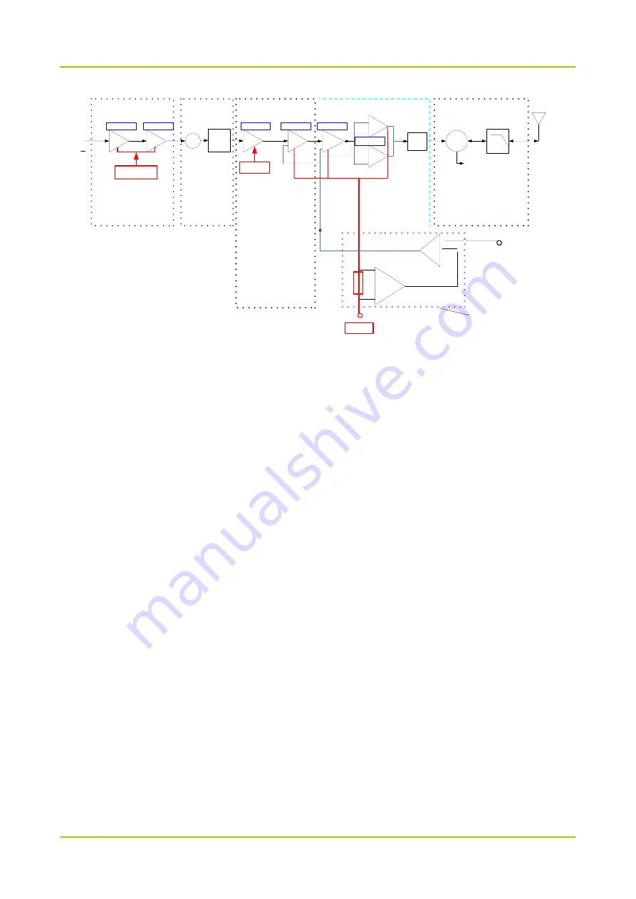
RF Power Amplifier Circuit
The carrier signal generated by TX VCO is modulated and amplified by 2SC5108/2SC3356, then goes to
the transmitter circuit through TX/RX
75
switch circuit. The signal passes through a π-type attenuator
first, allowing interstage isolation between the RF power amplifier circuit and TX VCO. After that, the
signal goes to the pre-driver amplifier (2SC3356) for pr
H
amplification, allowing
DQ
interstage isolation between the pre-driver amplifier and the next amplifier. Then, the signal goes to
another pre-driver amplifier (BFQ540) and the driver amplifier (2SK3078) for further power amplification,
to provide
DGHTXDWHO\DPSOLILHG
signal to the final-stage amplifier (RFM03U3CT) for final power
amplification. After amplified by multiple amplifiers, the signal will pass through a microstrip matcher to
complete output impedance matching, so as to reduce output power loss due to impedance mismatch.
Then the transmitting signal will go to the low-pass filter through TX/RX switch circuit.
Low-pass Filter Circuit (for suppressing harmonics)
The low-pass filter for suppressing harmonics is a high-order Chebyshev filter composed of
lumped-parameter inductors and capacitors. Via this filter, the spurious signal within the stop band can
be attenuated as much as possible while the in-band ripple is within the required range.
Auto Power Control Circuit
In the auto power control circuit, the drain current from the driver amplifier and final-stage amplifier is
converted to voltage via the sampling resistor and subtraction circuit (composed of the first operational
amplifier). This voltage is compared with the APC control voltage (output by DAC) at the second
operational amplifier. Then the error voltage, which is output by the second operational amplifier,
controls TX power by controlling the bias voltage at the gates of the amplifiers (including the driver
amplifier 2SK3078 and the final-stage amplifier).
Summary of Contents for PD362
Page 1: ...PORTABLE ...
Page 5: ...Ua 400 440 MHz ...
Page 16: ...Ua 400 440 MHz Exploded View and Packaging Guide 9 3 2 Packaging Guide ...
Page 43: ...9 PCB View Main Board_Top Layer 35 ...
Page 44: ...Main Board_Bottom Layer 36 ...
Page 73: ...Uc 430 470 MHz ...
Page 84: ...Uc 430 470 MHz Exploded View and Packaging Guide 9 3 2 Packaging Guide ...
Page 111: ...9 PCB View Main Board_Top Layer 35 ...
Page 112: ...Main Board_Bottom Layer 36 ...


