


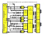


DP-4X MAIN and SUB SYNC CIRCUIT DIAGRAM EXPLANATION
PAGE 03-13
(Continued from page 12)
I501 SUB Y Pr/Pb Selector Sync Inputs and Outputs:
Any signal that have been selected for the Sub Picture, is selected by this IC via I
2
C communications to the Mi-
croprocessor
SDA2
pin
3
and
SCL2
pin
4
.
It selects the following; 1H NTSC, Component Inputs, ATSC Tuner (Not in the DP-43 Chassis), and
HDMI.
I501 Inputs:
This IC Receives the following 4 types of Inputs;
1.
1H NTSC:
The outputs from
IV12
are received by
I501
. They will be either the Sub Tuner, Com-
posite Video 2, 3, 4 or 5, S-In 3, 4 or 5, Component NTSC Y Pr/Pb. Any of these inputs that have
been selected by
IV12
are received by
I501
on the following pins;
Y
pin
66
,
Cb
pin
68
and
Cr
pin
70
.
2.
Component 1 or 2, HDMI 1 Inputs: I501
receives the Component 1 or 2 and/or HDMI 1 inputs at
the following pins,
Y
pin
78
,
Pb
pin
80
and
Pr
pin
2
.
3.
ATSC (Digital Tuner) Inputs: I502
receives the Digital Tuner (1080i) inputs at the following
pins,
Y
pin
72
,
Pb
pin
74
and
Pr
pin
76
. Not in the DP-43 Chassis. (Not in the DP-43 Chassis),
I501 Sub H and V Sync Outputs
;
Dependant upon the Customer’s selection for the Sub Picture,
I501
outputs the sync signals on the fol-
lowing pins;
H Sync
pin
19
and
V Sync
pin
17
. These are input to
I503
.
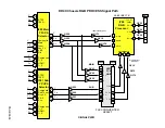
SUB SYNC IN AND OUT OF I503 SYNC INVERTER:
The H and V Sync arriving at pins
13
and
11
of
I503
are routed through inverters. H. Sync is inverted
once to match the requirements of the Flex Converter/PinP Module.
V. Sync is inverted twice.
The H Sync is output pin
12
. The V Sync is output pin
8
.
SUB PICTURE SYNC INTO THE FLEX CONVERTER/PinP MODULE UY01:
H Sync is input to pin
15
of the
PFC1
connector and into the Flex Converter/PinP Module.
V Sync is input to pin
14
of the
PFC1
connector and into the Flex Converter/PinP Module.
SUB PICTURE FROM THE FLEX CONVERTER UY01 TO THE RAINFOREST IC IY04
The Sub Picture (if selected) is then added to the Main picture Y Pr/Pb signals inside the Flex Con-
verter/PinP Module and output along with the Main Pictures signal paths.
Summary of Contents for 51F510
Page 2: ...DP 4X BLANK PAGE NOTES BLANK PAGE ...
Page 5: ...DP 4X CHASSIS INFORMATION POWER SUPPLY INFORMATION SECTION 1 ...
Page 6: ...DP 4X BLANK PAGE NOTES BLANK PAGE ...
Page 30: ...DP 4X BLANK PAGE NOTES BLANK PAGE ...
Page 31: ...DP 4X CHASSIS INFORMATION MICROPROCESSOR INFORMATION SECTION 2 ...
Page 32: ...DP 4X BLANK PAGE NOTES BLANK PAGE ...
Page 44: ...DP 4X BLANK PAGE NOTES BLANK PAGE ...
Page 45: ...DP 4X CHASSIS INFORMATION VIDEO INFORMATION SECTION 3 ...
Page 46: ...DP 4X BLANK PAGE NOTES BLANK PAGE ...
Page 61: ...DP 4X CHASSIS INFORMATION AUDIO INFORMATION SECTION 4 ...
Page 62: ...DP 4X BLANK PAGE NOTES BLANK PAGE ...
Page 66: ...DP 4X BLANK PAGE NOTES BLANK PAGE ...
Page 67: ...DP 4X CHASSIS INFORMATION DEFLECTION INFORMATION SECTION 5 ...
Page 68: ...DP 4X BLANK PAGE NOTES BLANK PAGE ...
Page 79: ...DP 4X CHASSIS INFORMATION DIGITAL CONVERGENCE INFORMATION SECTION 6 ...
Page 80: ...DP 4X BLANK PAGE NOTES BLANK PAGE ...
Page 94: ...DP 4X BLANK PAGE NOTES BLANK PAGE ...
Page 95: ...DP 4X CHASSIS INFORMATION CHASSIS PICTURES SECTION 07 ...
Page 96: ...DP 4X BLANK PAGE NOTES BLANK PAGE ...
Page 104: ...DP 4X BLANK PAGE NOTES BLANK PAGE ...
Page 105: ...DP 4X CHASSIS INFORMATION DP 4X CHASSIS ADJUSTMENTS SECTION 08 ...
Page 106: ...DP 4X BLANK PAGE NOTES BLANK PAGE ...
Page 108: ...DP 4X BLANK PAGE NOTES BLANK PAGE ...
Page 144: ...DP 4X BLANK PAGE NOTES BLANK PAGE ...
Page 146: ...DP 4X BLANK PAGE NOTES BLANK PAGE ...
Page 147: ...DP 4X CHASSIS INFORMATION SERVICE POLICY FOR THE DP 4X CHASSIS SECTION 10 ...
Page 148: ...DP 4X BLANK PAGE NOTES BLANK PAGE ...
Page 151: ...DP 4X BLANK PAGE NOTES BLANK PAGE ...
Page 152: ...DP 4X BLANK PAGE NOTES BLANK PAGE ...


